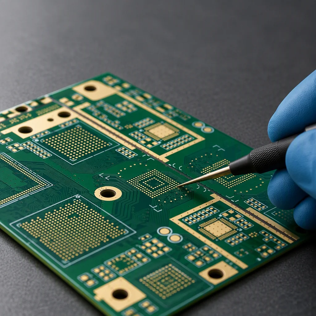
Pre-submission checklist
The DFM checklist to clear before you send files
Seven stages, the numeric limit that applies to each, and the two items that have to be confirmed against your own project rather than assumed from a table.
How to use this list
Free before the PO, expensive after it
Design-for-manufacture review is free before a purchase order and expensive after one. This is the list we run internally, arranged in the order a fabrication and assembly quotation is actually reviewed: stackup, copper, drills, mask and legend, panelisation, placement and thermal limits, then test access. Work down it once and most of the questions that would otherwise arrive mid-production are already answered.
Two kinds of entry appear below. Most carry a number fixed by the process, a 0.2 mm mechanical drill, a 0.1 mm solder-mask web, a 6 mil cost-optimal trace and space. A few are marked confirmed per project, because the answer genuinely depends on your build: aspect ratio, and the maximum board size an SMT line will accept. Those are written that way on purpose. A checklist that invents a number is worse than no checklist, because it moves the discovery to the first production panel.
Send Gerber in RS-274X or 274D, ODB++ or IPC-2581, together with the BOM and the pick-and-place file, and the review comes back inside 24 hours with the quotation. There is no MOQ, so the same review applies to five boards or fifty thousand.
Stage 1, Stackup
Layers, thickness and laminate
Start with the structure, because everything downstream is constrained by it. Layer count sets the fabrication route and the price band before any geometry is discussed.
- Layer count: 1–58 layers; 2–8 is the volume standard, 10–20 and HDI are quoted per project
- Finished thickness 0.4–3.2 mm; copper 0.5–20 oz, heavy copper from 3 oz (105 µm) to 20 oz (700 µm)
- High-Tg FR-4 at ≥170 °C wherever the assembly is lead-free; FR-4 from Tg 130–180 °C for the rest
- Controlled-Dk laminates: Rogers RO4350B (Dk 3.48 (specified as an absolute tolerance by the laminate supplier)), Isola 370HR (Dk 4.04), Megtron 6 (Dk 3.40)
- Panel limit: 600 × 1200 mm maximum laminate size, the boundary your array has to fit inside
Stage 2, Copper
Trace, space and what impedance costs
Minimum geometry is where a design either sits inside the cost-optimal window or leaves it. There is no penalty for staying at 6 mil; there is a price step for going below it.
- Trace and space: 6 mil (0.15 mm) is the cost-optimal standard. HDI builds go down to 2.5 mil.
- Impedance: ±10% is the standard tolerance and ±5% is available on premium builds, both verified by a TDR test coupon at the board edge. The coupon needs board area and panel space, so it belongs in the array plan rather than in a change order.
- Differential pairs: controlled to 100 Ω.
- Annular ring: 0.15 mm (6 mil) minimum.
- Aspect ratio: confirmed per project, because it depends on the finished thickness and the smallest drill in the same stackup rather than on a single published figure.
Stage 3, Drills and vias
Holes, microvias and via-in-pad
Drill sizes decide the fabrication route, the annular ring budget and the price. They also decide whether a BGA pad can be flat enough to print on.
- Mechanical drill: 0.2 mm minimum.
- Laser microvia for HDI: 0.1 mm (4 mil) minimum.
- Via fill: conductive epoxy, non-conductive epoxy, tented or plugged. Where a via-in-pad sits under a BGA or a fine-pitch part, specify it plugged and capped, so the paste volume on that pad is predictable rather than a function of the hole.
- Edge features: plated edges and castellated half-holes are both available, and both change the outline data and the array.
- Aspect ratio: confirmed per project, as above. It is the ratio between the smallest drill and the finished thickness.
Stage 4, Mask and legend
Solder mask, silkscreen and fiducials
Mask and legend are the two layers most often treated as cosmetic and most often responsible for a first-article surprise.
- Solder-mask web: 0.1 mm minimum between pads. Below that the mask lifts or bridges, and the assembly inherits the defect as a short.
- Mask colour: green, red, yellow, blue, white or black. One colour per order, checked for consistency across the batch.
- Silkscreen: 0.15 mm minimum line width and 0.8 mm minimum character height, a 1:5 ratio. Keep legend off pads, test points and fiducials.
- Fiducials: the placement vision system has to find them. Provide a global set for the array and local fiducials for fine-pitch parts; size, clearance and contrast are confirmed per project against the machine's field of view.
- Reference designators: keep them legible at 0.8 mm character height as well, because AOI and human final inspection both read them.
Stage 5, Panel
Panelisation, tabs and breakaway
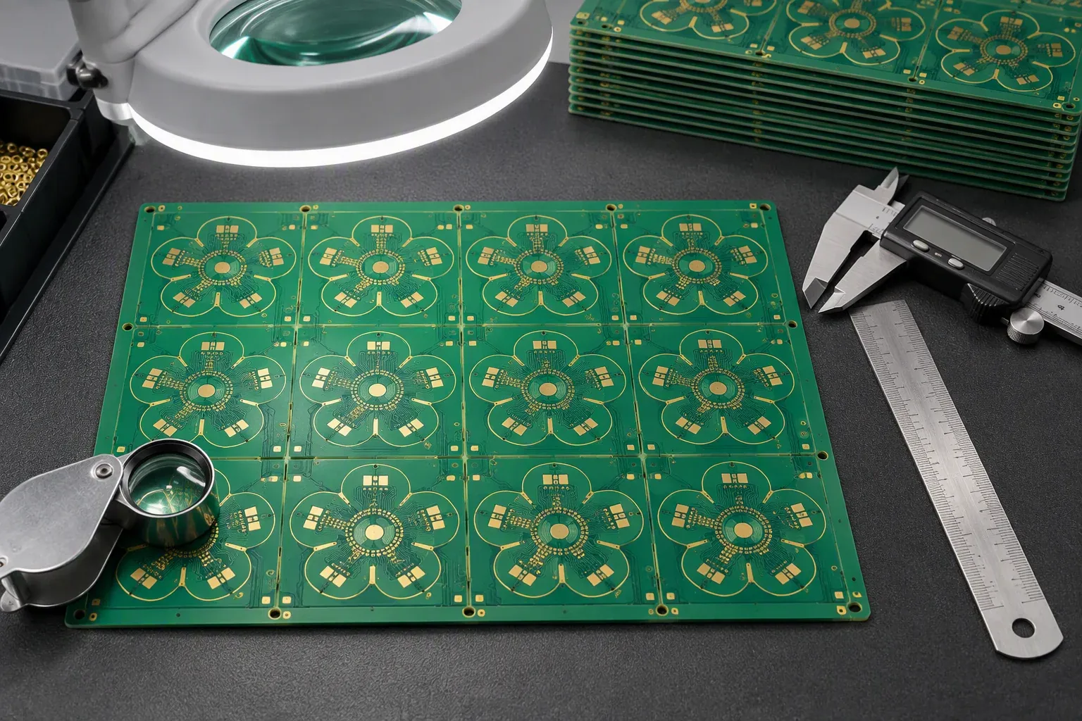
The array is where cost, breakaway quality and machine handling meet, and where a 0.1 mm decision changes the price of the whole order.
- Array design: measured against 600 × 1200 mm maximum laminate size first, then against the SMT line limit.
- SMT line board limit: confirmed per project. Conveyor-class lines typically accept 510 × 460 mm.
- Breakaway tabs and V-score lines have to stay clear of components, test points and connectors, and the router path has to respect the 0.2 mm minimum mechanical drill.
- Edge rails carry the panel through printing and placement. They are tooling rather than product, so keep shipping circuitry off them.
- Panelisation also decides how much laminate you pay for, which makes it one of the largest cost levers available before a single board is built.
Stage 6, Placement and heat
Component limits and thermal relief
This is the stage where a mechanical decision, a tall capacitor, a heatsink, a ground plane, turns into a soldering problem, and it is cheaper to find that in the checklist than on the line.
- Component range: 01005 and 0201 passives upward; BGA to 0.25 mm pitch; fine pitch to 0.3 mm; maximum component height 25 mm on the SMT side.
- Wave-soldering clearance: 120 mm above the board and 15 mm below it. A tall electrolytic or a heatsink can block an entire through-hole route.
- Thermal relief: ground and plane connections on through-hole pins need relief or a deliberate heat path, or hand and selective soldering cannot reach temperature. Under a power device, thermal vias in the pad are the usual answer.
- Reflow: 8–12 zones with a lead-free peak of 245–260 °C, paired with high-Tg laminate at ≥170 °C.
- Moisture: MSL floor life is a design input as well, 168 hours at MSL3 down to 24 hours at MSL5a, with a 125 °C bake of about nine hours for saturated MSL3 parts with bodies of 1.4 mm or less.
Stage 7, Test access
Probe points and documentation
Test coverage is designed in layout, not added in production. A node with no accessible point is a node that gets verified by functional test or not at all.
- ICT: up to 3,072 test points. Any node you want tested needs a probe point, a via or a pad of usable size, placed on a grid a fixture can reach.
- Flying probe: four heads, no fixture, fast to program and slower per unit, the right route for prototypes and low volume.
- AOI: 100% of boards on every SMT line, which is another reason to keep polarity marks and designators legible.
- X-ray: a minimum of five boards per lot on hidden joints, so any BGA, QFN or LGA design should plan for it.
- Documentation: CoC, test report with ICT and FCT pass records, RoHS and REACH material declarations, packing list and commercial invoice travel with the goods; FAI reports, AOI and X-ray images and SPI data are available on request.
One-page summary
The whole checklist in one table
| Stage | Check | Limit or value |
|---|---|---|
| Stackup | Layer count | 1–58 layers; 2–8 volume standard, 10–20 and HDI per project |
| Stackup | Finished thickness | 0.4–3.2 mm |
| Stackup | Copper weight | 0.5–20 oz; heavy copper from 3 oz (105 µm) |
| Stackup | Laminate for lead-free reflow | High-Tg FR-4, Tg ≥170 °C |
| Stackup | Maximum laminate size | 600 × 1200 mm |
| Copper | Minimum trace and space | 6 mil (0.15 mm) standard; 2.5 mil on HDI |
| Copper | Impedance tolerance | ±10% standard, ±5% premium; TDR coupon at the board edge |
| Copper | Annular ring | 0.15 mm (6 mil) minimum |
| Copper | Aspect ratio | Confirmed per project |
| Drills | Mechanical drill | 0.2 mm minimum |
| Drills | Laser microvia (HDI) | 0.1 mm (4 mil) minimum |
| Drills | Via-in-pad | Plugged and capped; conductive or non-conductive epoxy fill |
| Drills | Edge plating, castellated holes | Available; outline data and array must account for them |
| Mask | Solder-mask web | 0.1 mm minimum |
| Legend | Silkscreen | 0.15 mm line width, 0.8 mm character height (1:5) |
| Fiducials | Array and local fiducials | Size, clearance and contrast confirmed per project |
| Panel | SMT line board limit | Confirmed per project; conveyor-class lines typically 510 × 460 mm |
| Panel | Breakaway tabs, V-score, edge rails | Clear of components, test points and connectors; router respects 0.2 mm drill |
| Placement | Component range | 01005 up; BGA to 0.25 mm pitch; fine pitch to 0.3 mm; height ≤25 mm |
| Thermal | Wave-solder clearance | 120 mm above the board, 15 mm below |
| Thermal | Reflow peak, lead-free | 245–260 °C over 8–12 zones |
| Thermal | MSL floor life | MSL3 168 h · MSL4 72 h · MSL5 48 h · MSL5a 24 h |
| Test | ICT access | Up to 3,072 test points (Agilent i3070) |
| Test | X-ray sampling | Minimum 5 boards per lot |

Free DFM review before the PO
Send the files and get the list run
An engineer walks your Gerber, BOM and pick-and-place through these stages and replies inside 24 hours with a quotation, a DFM report and the items that need a decision. No MOQ.