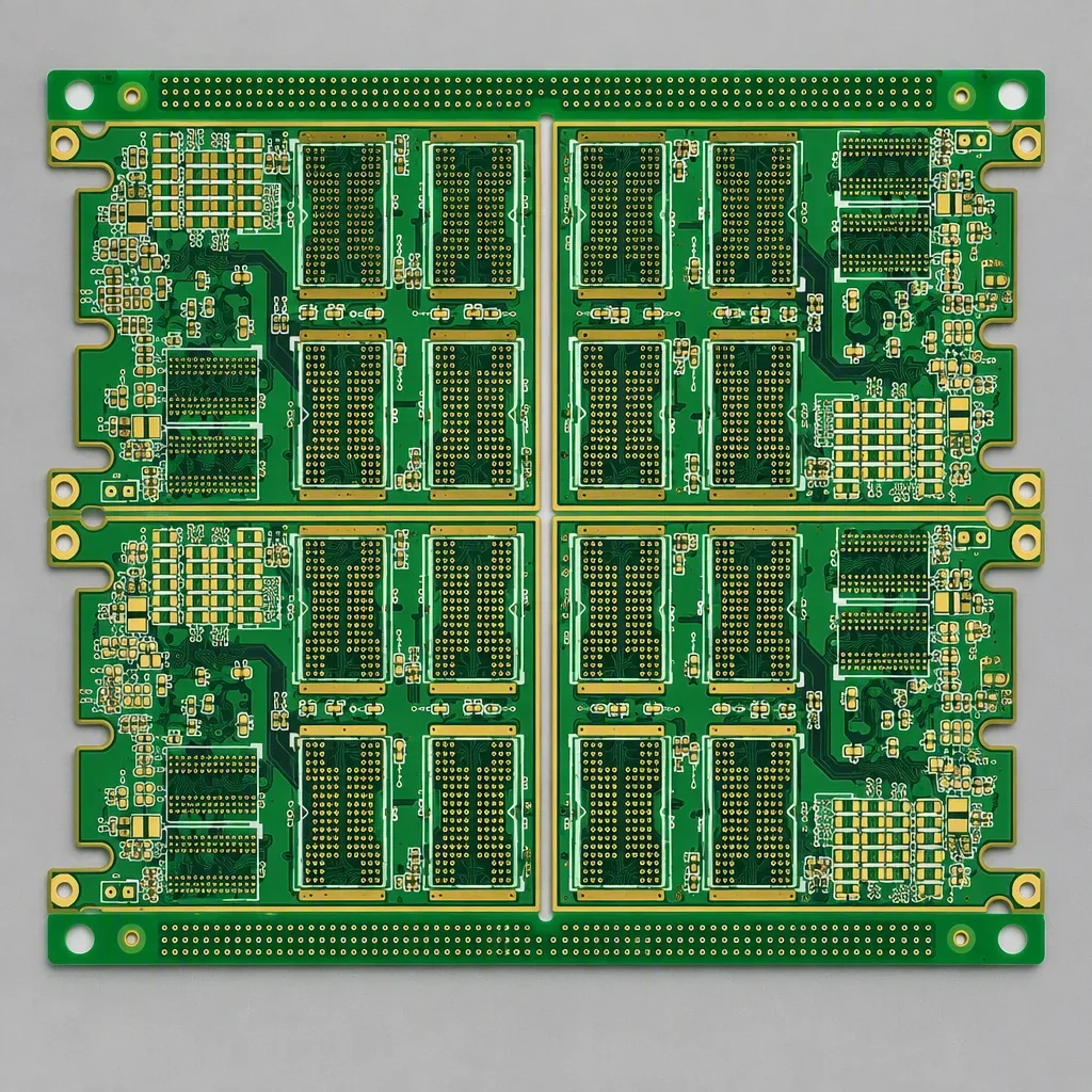
Green
The default across nine SMT lines and the colour every AOI recipe is tuned on first, so contrast against gold and tin is a known quantity.
Materials & surface finishes
Six laminate families, eight surface finishes and six solder-mask colours. Every row below carries the thickness range it is held to, the process window it belongs in, and the reason to choose it over the row above.
Laminate comparison
Tg decides whether a board survives the 245–260 °C peak of lead-free reflow. Dk decides what happens to a trace once the signal passes 1 GHz. Read the row that matches your constraint, not the row with the longest datasheet.
| Laminate | Tg | Dk (nominal) | Df (nominal) | Typical use |
|---|---|---|---|---|
| FR-4, standard | 130–180 °C | Per datasheet | Per datasheet | Cost-led digital and analog boards, 2–8 layers laminated in-house |
| High-Tg FR-4 | ≥170 °C | Per datasheet | Per datasheet | Lead-free reflow, thermal cycling, automotive-grade documentation |
| Rogers RO4350B | Per datasheet | 3.48 (specified as an absolute tolerance by the laminate supplier) | Per datasheet | RF, antenna feeds and impedance-critical 50 Ω runs |
| Taconic (PTFE / woven glass) | Per datasheet | Per datasheet | Per datasheet | Low-loss RF above 1 GHz, radio front ends and radar boards |
| Aluminium IMS | Metal base | Per datasheet | Per datasheet | LED and power boards where the board itself is the heatsink |
| Polyimide (FPC / rigid-flex) | Per datasheet | Per datasheet | Per datasheet | Flex and rigid-flex builds that bend in service and in assembly |
“Per datasheet” marks a value that belongs to the exact grade, thickness and copper weight you order, so we quote it from the laminate supplier’s datasheet in the DFM reply instead of printing a generic figure. Three grades on the approved list already carry published values at the laminate level: Rogers RO4350B at Dk 3.48 (specified as an absolute tolerance by the laminate supplier), Isola 370HR at Dk 4.04 and Megtron 6 at Dk 3.40. Board thickness runs 0.4–3.2 mm, copper weight 0.5–20 oz, minimum mechanical drill 0.2 mm and minimum laser microvia 0.1 mm (4 mil) on HDI builds.
Surface finish matrix
The finish decides solderability, shelf life and how flat a pad stays at 0.25 mm pitch. Thicknesses below are the specification the shop works to, not a marketing range, and every row states the constraint that comes with it.
| Finish | Thickness | Choose it when | Constraint to plan for |
|---|---|---|---|
| HASL, lead-free | 1–40 µm | General-purpose boards and cost-led programmes | RoHS-compatible, but the surface is not perfectly planar after the hot-air levelling pass |
| HASL, leaded | 1–25 µm | Legacy assemblies that stay on a tin-lead process | Cannot be released on a RoHS-only build, the alloy is tin-lead |
| ENIG (immersion gold) | Ni 3–6 µm + Au 0.05–0.1 µm per IPC-4552 |
BGA, fine pitch and RF, the flattest solderable surface we run | Costs more than HASL, and the nickel–gold chemistry has to stay in control to avoid black pad |
| ENEPIG | Ni 3–6 + Pd 0.05–0.1 + Au 0.03–0.05 µm | High-reliability builds and wire-bondable pad finishes | Highest cost tier in the table; specify it only where bonding actually demands it |
| OSP (organic solderability preservative) | Film 0.2–0.5 µm, 6-month shelf life | Planar, halogen-free finishing on a simple process chemistry | The film is consumed by every reflow pass, so plan the number of thermal excursions |
| Immersion silver | Per supplier datasheet | Fine-pitch SMT and press-fit connectors | Tarnishes in air. Keep the board in its sealed bag until the line is ready |
| Immersion tin | Per supplier datasheet | Fine-pitch SMT and press-fit work | Whisker-controlled storage; confirm the supplier’s shelf-life statement per lot |
| Hard gold (gold finger) | 150–200 HK25, rated for >10,000 mating cycles | Edge connectors and PCIe-style card fingers | Applied to the finger area only, it is not a whole-board finish |
Solder mask
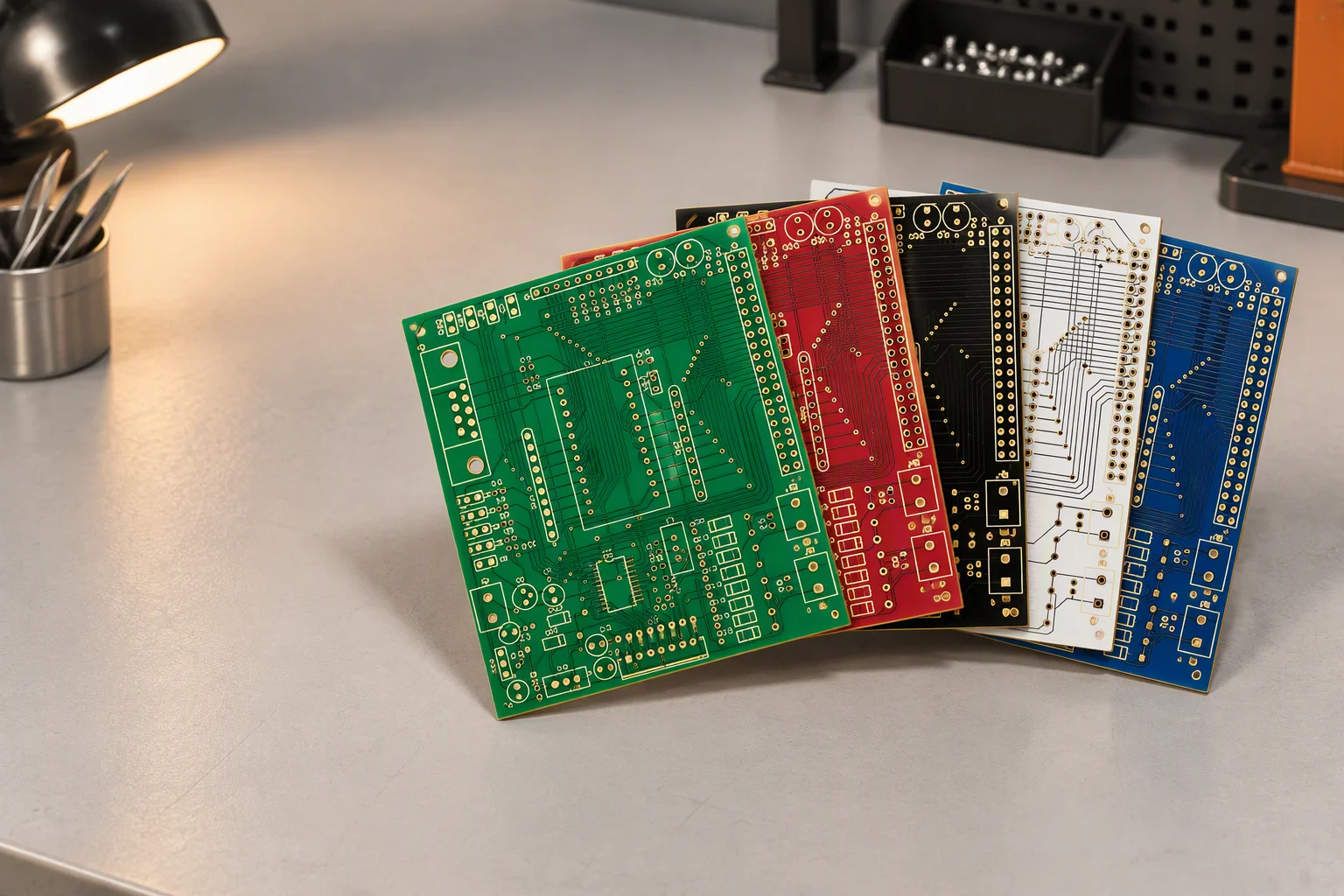
Green, red, yellow, blue, white and black are all stocked, and colour costs nothing to change. The fabrication limits do not move: a 0.1 mm minimum solder-mask web between adjacent pads, and silkscreen no finer than 0.15 mm wide and 0.8 mm high at a 1:5 stroke-to-height ratio. The five boards photographed below are five real production boards (a sixth colour, yellow, is available but not pictured here, so they are not one artwork in five masks; they are five different designs). Compare artwork in five colours under identical light.
The default across nine SMT lines and the colour every AOI recipe is tuned on first, so contrast against gold and tin is a known quantity.
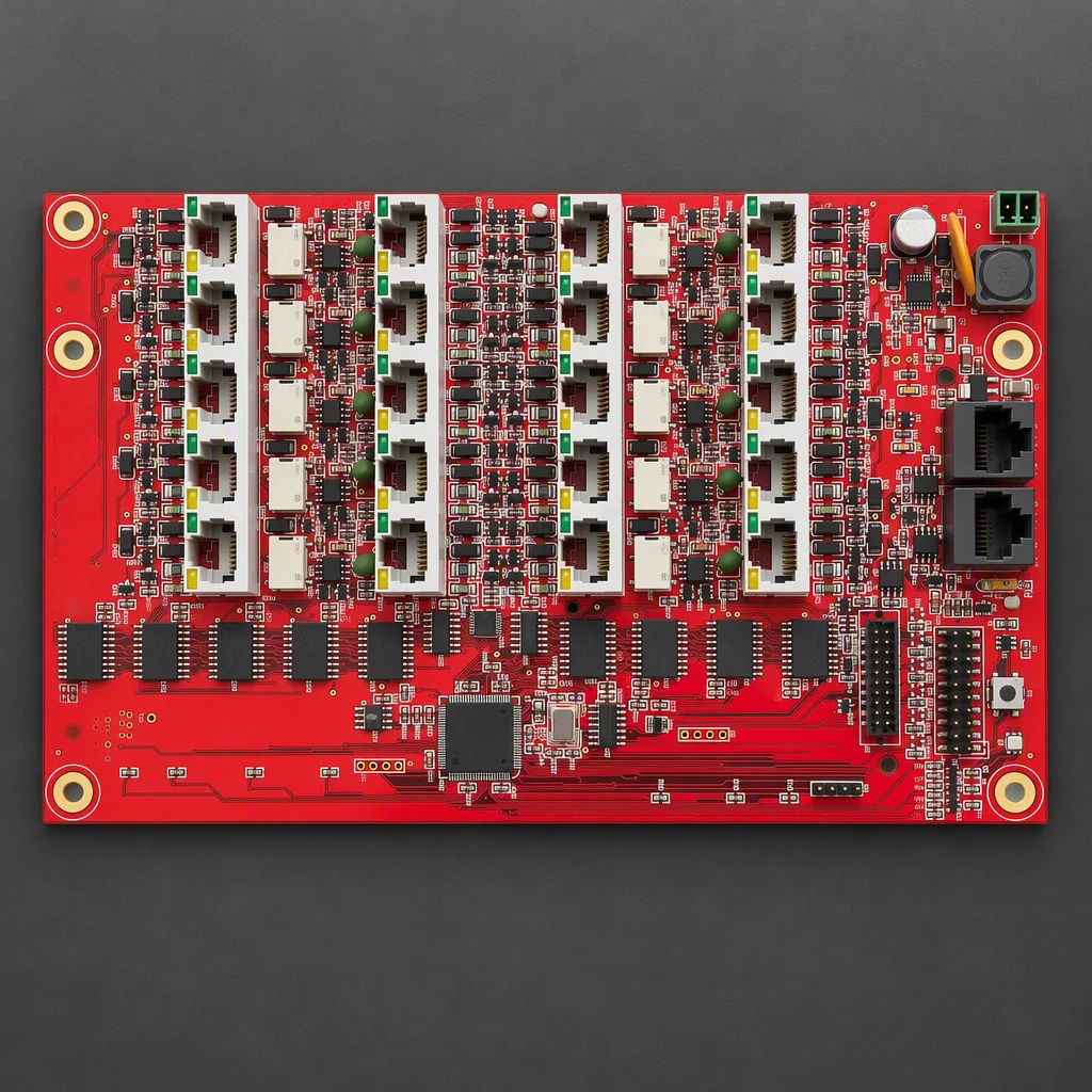
Common on industrial control boards where a service technician identifies a product family from across a cabinet, with no label to read.
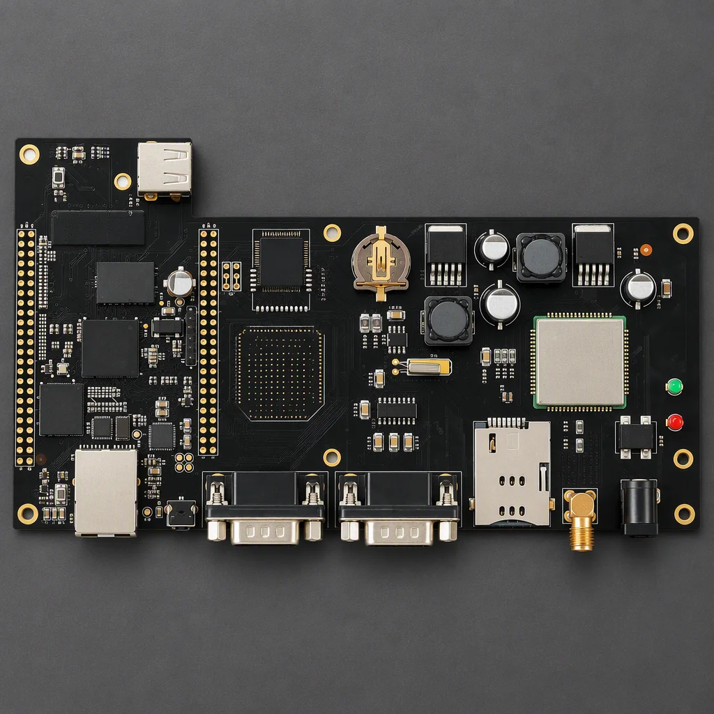
Hides copper shading on dense layouts. Final visual inspection runs under the same IPC-A-610 Class 2 & 3 workmanship lighting as every other colour.
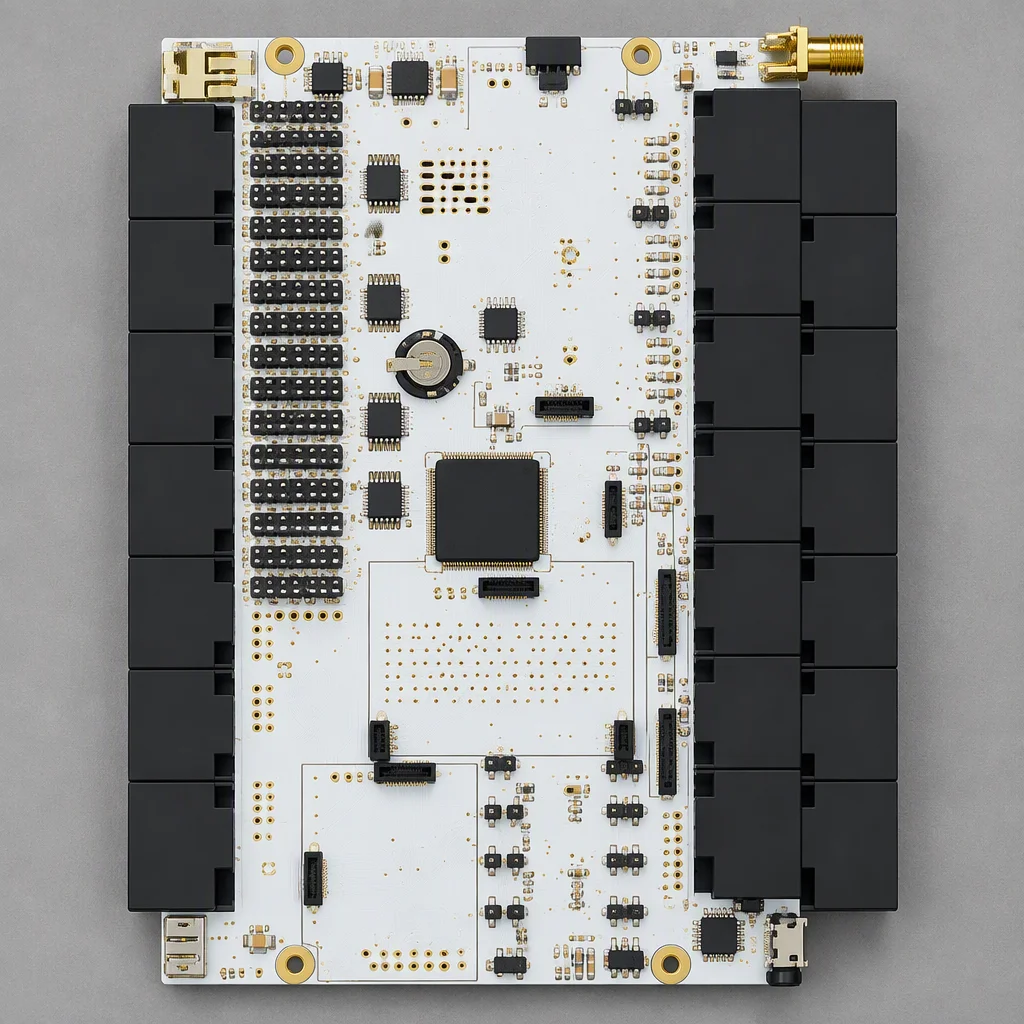
Frequent on LED and power boards. White shows every trace of flux residue, so it is normally paired with the ultrasonic and DI-water clean.
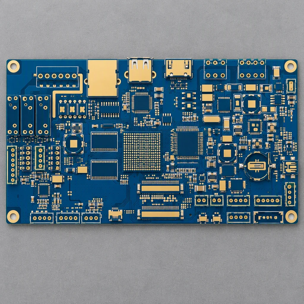
Used where a customer colour-codes a product line. Electrical and fabrication limits are identical to green, only the pigment changes.
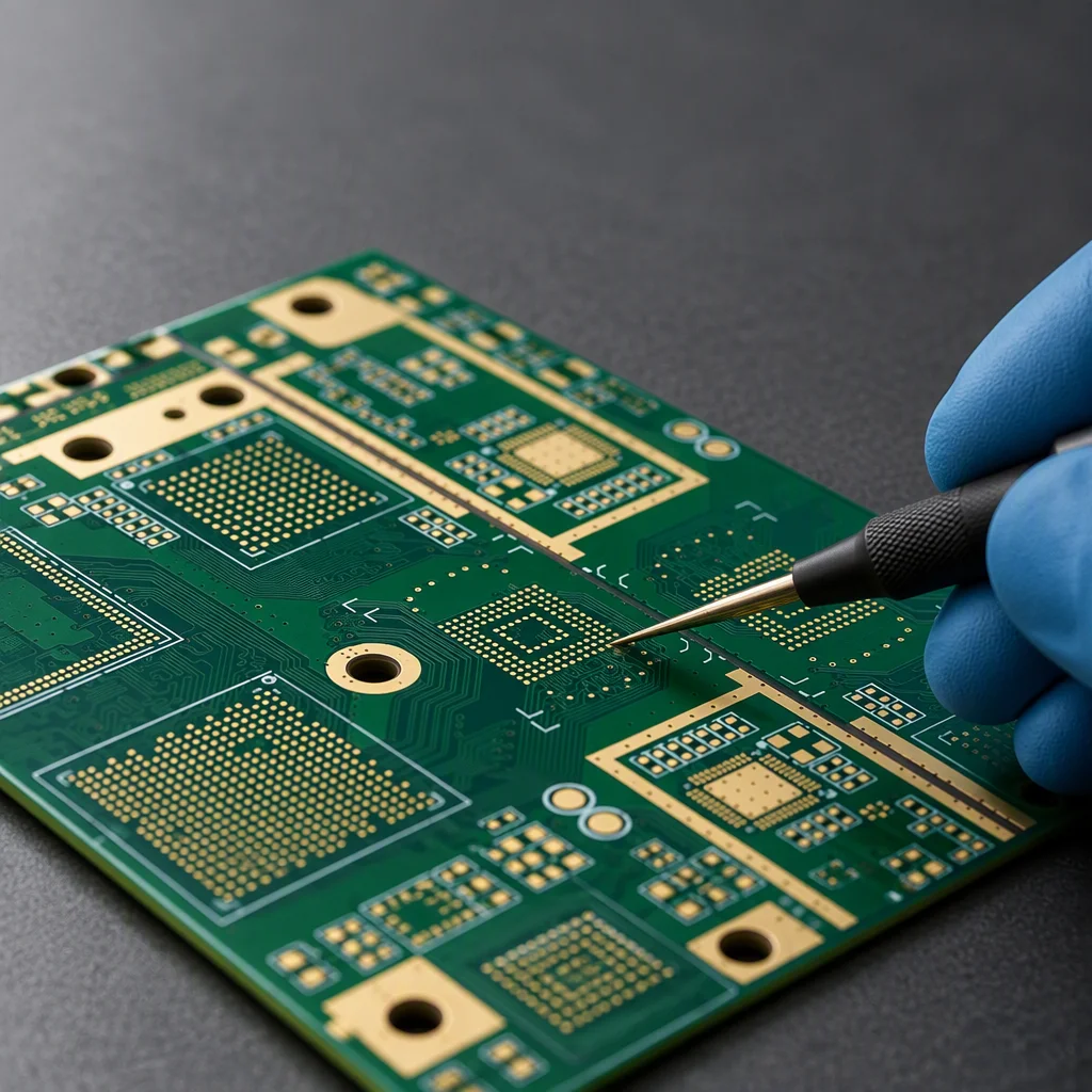
Finish close-up
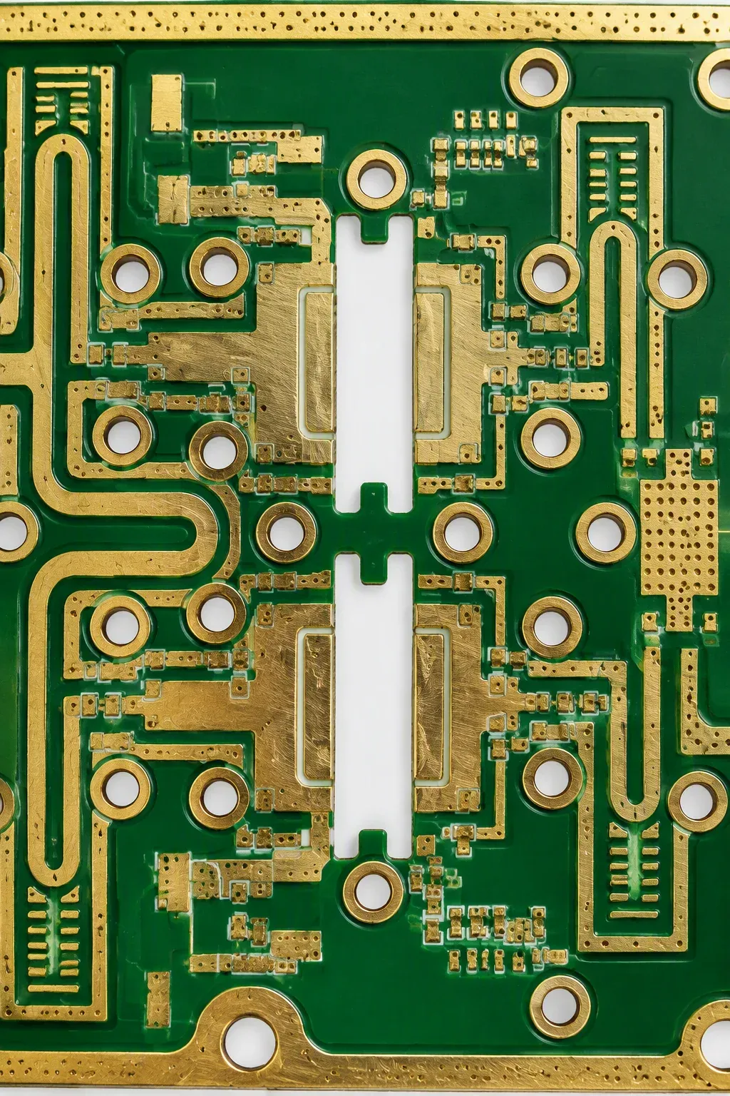
Flatness is the entire argument for ENIG. A nickel barrier under a thin gold layer keeps the pad coplanar, so a 0.25 mm-pitch BGA lands on paste rather than on a solder bump left behind by hot-air levelling.
Selection criteria
Six requirements settle almost every laminate-and-finish question that reaches the DFM desk. Match your row and the material follows.
Compliance & declarations
Material selection is also an audit question. These are the statements we can put on file for a build, in the wording a compliance engineer can actually use.
Selection flow
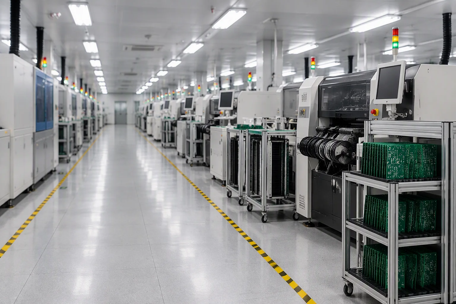
Nothing is laminated until gate four clears. The stackup, the laminate and the finish are confirmed against your impedance target before the first panel is etched, and the quotation lands inside 24 hours of gate one.
Send it to the DFM desk
Layer count, laminate family, finish, mask colour and impedance target are enough for an engineer to answer properly, engineering review and quotation within 24 hours.
Send your Gerber, BOM or a plain description. An engineer, not a sales script, reviews it and replies within one working day. NDA on request.