Multilayer & HDI
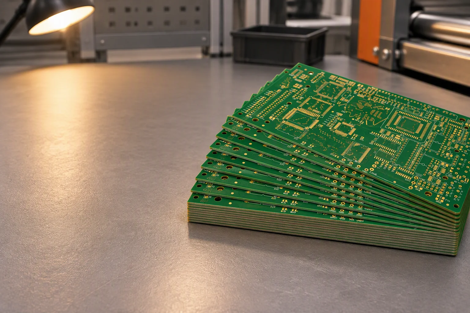
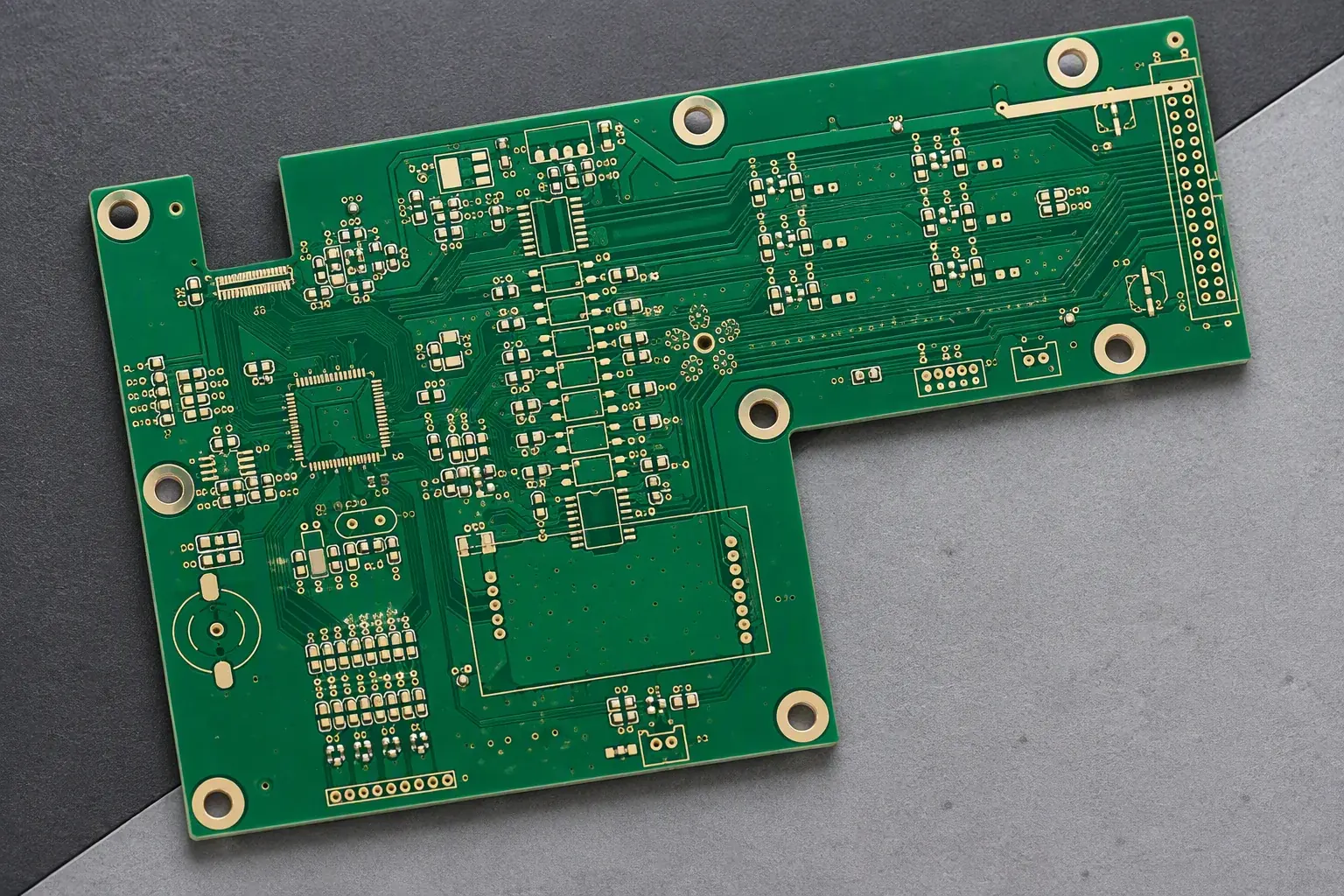
Sequential lamination, blind and buried vias, via-in-pad filling and back-drilling, with impedance held to ±10% standard and ±5% on premium builds, both verified by TDR coupons on the panel border.
Multilayer & HDIPCB fabrication
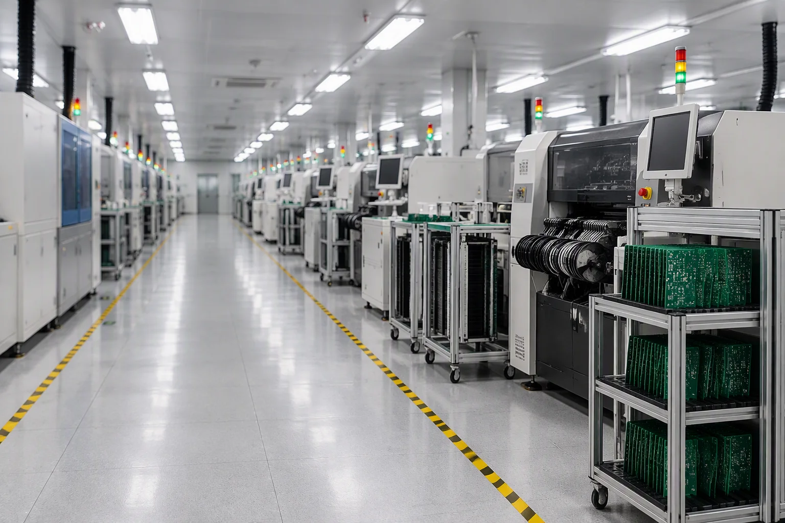
Imaging, lamination, drilling, plating and surface finish all happen on this site. Nothing is placed out to a second board shop. Lines and spaces go down to 2.5 mil on HDI, laser microvias to 0.1 mm, panels up to 600 × 1200 mm, and the quotation with its DFM report comes back inside 24 hours.
Find your layer class
Layer count decides the lamination cycles, the drill programme and the inspection plan. Locate your board in the table, then read across to see what the tier normally implies.
| Layer class | Construction | Typical use | Decisive process |
|---|---|---|---|
| Single & double sided | 1–2 copper layers, 0.4–3.2 mm board, 1–20 oz copper | Power entry, LED carriers, simple control and sensor boards | Punching or routing, HASL or OSP, one drill programme at 0.2 mm minimum |
| 4–6 layers | One or two cores, 1–2 oz outer copper, standard FR-4 or high-Tg | Industrial control, consumer products, IoT gateways | Sequential lamination once, impedance control at ±10% standard on 50 Ω and 100 Ω nets |
| 8–20 layers | Multiple cores, back-drilling available, low-loss laminate on request | Telecom line cards, motor drives, instrumentation | Layer-to-layer registration, controlled-depth back-drill, TDR coupon on the panel border |
| HDI, 1+N+1 upward | Laser microvias at 0.1 mm, buried and blind vias, conductive or non-conductive fill | Handheld devices, wearables, dense BGA and CSP routing | Sequential lamination twice or more, via filling and planarisation, 2.5 mil lines on the outer layers |
| Advanced builds to 58 layers | Quoted per project: stackup, drill plan and impedance targets confirmed with your engineer | Backplanes, high layer-count test and computing hardware | Press-cycle control and anti-CAF material selection, verified by coupon and microsection |
Process limits
These are the production limits, not the laboratory ones. A design that respects every row below moves through the plant without a special-process waiver.
| Parameter | In-house limit | Notes |
|---|---|---|
| Layer count | 1 – 58 | 2–8 layers is the volume tier; 10–20 layers and HDI are quoted per project; advanced builds to 58 layers on request |
| Minimum line / space | 2.5 mil | HDI tier; 6 mil (0.15 mm) is the cost-optimised standard tier |
| Minimum laser microvia | 0.1 mm (4 mil) | Laser drilled and plated; conductive or non-conductive fill available |
| Minimum mechanical drill | 0.2 mm | Annular ring held to 0.15 mm (6 mil); drill-to-thickness ratio reviewed per stackup |
| Board thickness | 0.4 – 3.2 mm | Finished thickness after lamination and surface finish |
| Copper weight | 0.5 – 20 oz | Heavy copper starts at 3 oz (105 µm) and runs to 20 oz (700 µm) on the heavy-copper line |
| Maximum panel size | 600 × 1200 mm | Smaller working panels are costed on the 510 × 460 mm conveyor envelope |
| Thermal stress | 288 °C for 10 s | Solder-float screening to the UL 796 and IPC-6012 requirement |
Nine production stages
Every stage below runs under one roof in Xixiang. Because lamination, drilling and plating are not subcontracted, a stackup change is a schedule change rather than a new supplier conversation.
Dry film laminated, exposed and etched to 2.5 mil features, then automatically optically inspected before bonding.
Prepreg and copper foil stacked under press-cycle control; high-Tg and low-loss laminates run on the same presses.
Mechanical holes from 0.2 mm, laser-drilled microvias from 0.1 mm (4 mil) on HDI, plus controlled-depth back-drilling.
Electroless copper then panel plating builds the barrels; copper is built to the target weight, up to 20 oz.
Pattern plating, etching and strip resist, with annular ring held to 0.15 mm (6 mil) minimum.
Green, red, yellow, blue, white or black, with a minimum mask dam of 0.1 mm; legend to 0.15 mm stroke and 0.8 mm character height.
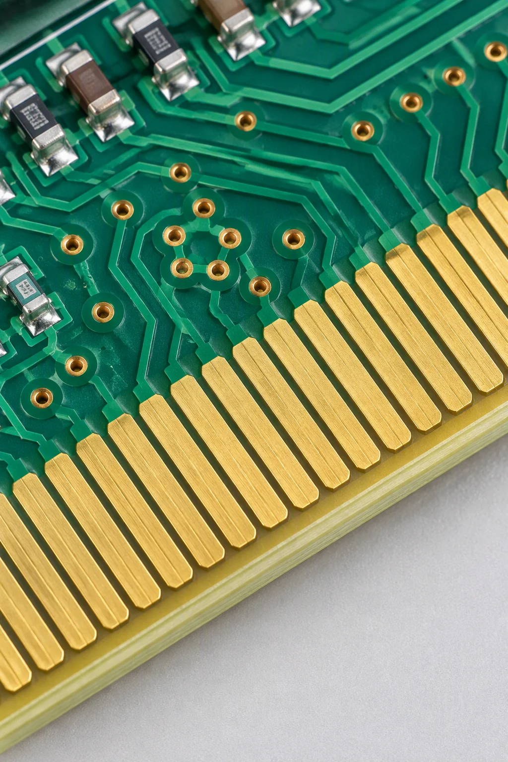
ENIG to IPC-4552, ENEPIG, HASL lead-free or leaded, OSP, immersion silver, immersion tin and hard gold on edge connectors.
Routing, V-scoring, edge plating and castellated half-holes, with gold-finger bevels set at engineering review against the connector's insertion count.
Flying probe on a Takaya APT-1500F for quick-turn work, ICT up to 3,072 points on an Agilent i3070 for volume, with a TDR coupon read on impedance-controlled builds.
Go deeper
Multi-layer construction, flexible substrates and surface chemistry each have their own limits and their own data. Open the page that matches the difficulty you are actually worried about.
Sequential lamination, blind and buried vias, via-in-pad filling and back-drilling, with impedance held to ±10% standard and ±5% on premium builds, both verified by TDR coupons on the panel border.
Multilayer & HDI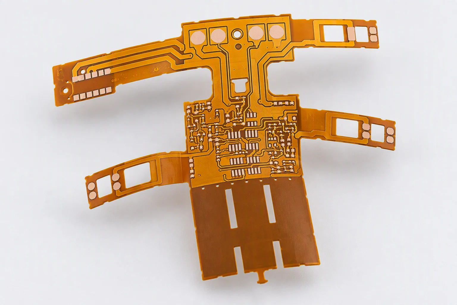
Polyimide cores with coverlay, adhesive and adhesiveless constructions, FR-4, polyimide or aluminium stiffeners, and panelisation with carriers so a flexible circuit can still cross an SMT line.
Flex & rigid-flex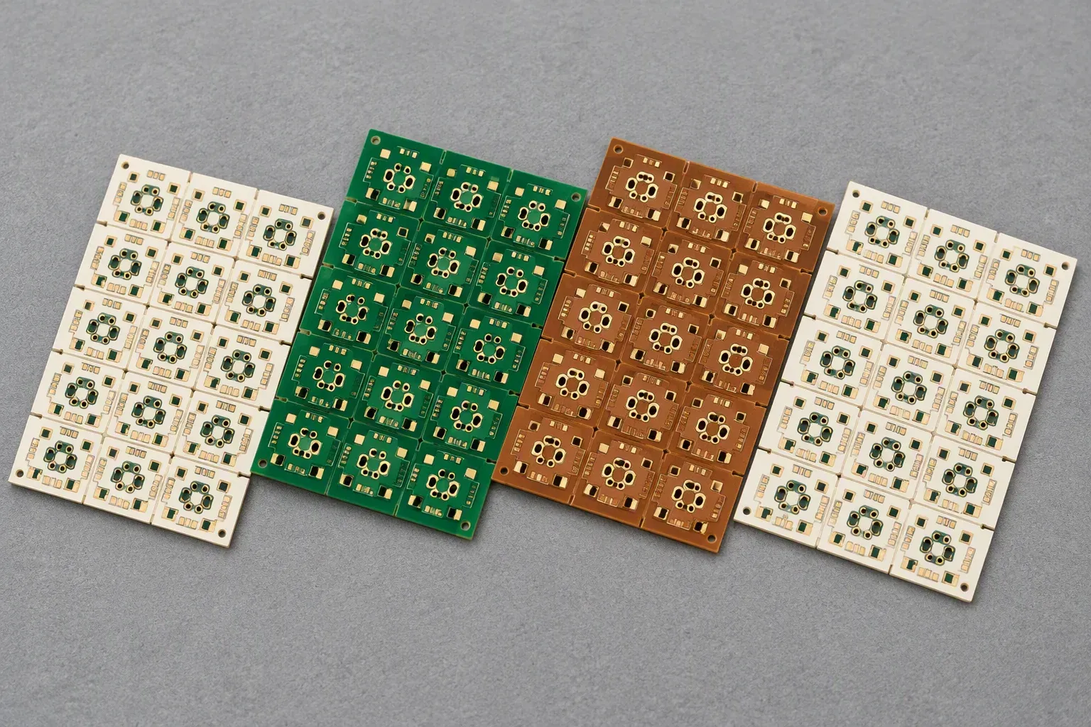
FR-4 to Tg 180 °C, high-Tg laminates above 170 °C, Rogers RO4350B at Dk 3.48, Isola 370HR, Megtron 6, Taconic, aluminium IMS and polyimide, matched to ENIG, ENEPIG, HASL, OSP, immersion silver or immersion tin.
Materials & finishesStructural features
These are the features that separate a routine board from one that needs an engineer attached to the order. All of them are standard work here, quoted from the same DFM review as everything else.
How the schedule is built
A date is only honest when it says whether the material is already on the shelf. Every quotation therefore carries two numbers: material in hand, and material still to be procured.
| Order tier | Bare-board window | What drives the date | How it is compressed |
|---|---|---|---|
| Prototype | 2 layers, under 50 pcs, under 1 m², 24 h | Layer count, the number of drill programmes and the surface finish | Lead-free HASL or OSP instead of ENIG, and a standard 0.15 mm line class |
| Small batch | 2/4 layers under 1 m², 5 days, 48 h expedited; 6/8 layers, 7 days; 10 layers and above, 10 days | Impedance requirements, back-drilling and the number of lamination cycles | Panelising several designs together, and confirming the stackup before the purchase order |
| Volume | Assembly 10–15 days, expedited 5–7 days | Component availability more than board capacity: standard FR-4 laminate is 6–8 weeks, MLCCs 20–50+ weeks, automotive MCUs and FPGAs 52+ weeks | Long-lead parts released early, or supplied on a consigned basis while boards start |
Files & DFM input
Send the data you already have. The DFM review is free and happens before any purchase order, so a missing detail costs a message rather than a re-run.
Quotation in 24 hours
Tell us the layer count, board size, surface finish and impedance targets. An engineer reviews the data and replies within one working day with a price and both lead-time brackets. NDA on request, and no part of your data is shared outside the project team.
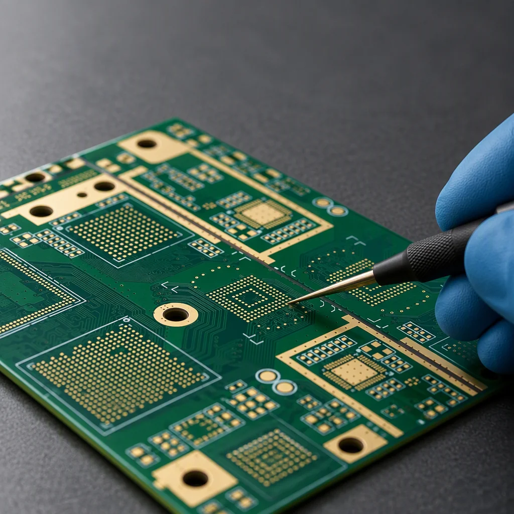
Send your Gerber, BOM or a plain description. An engineer, not a sales script, reviews it and replies within one working day. NDA on request.