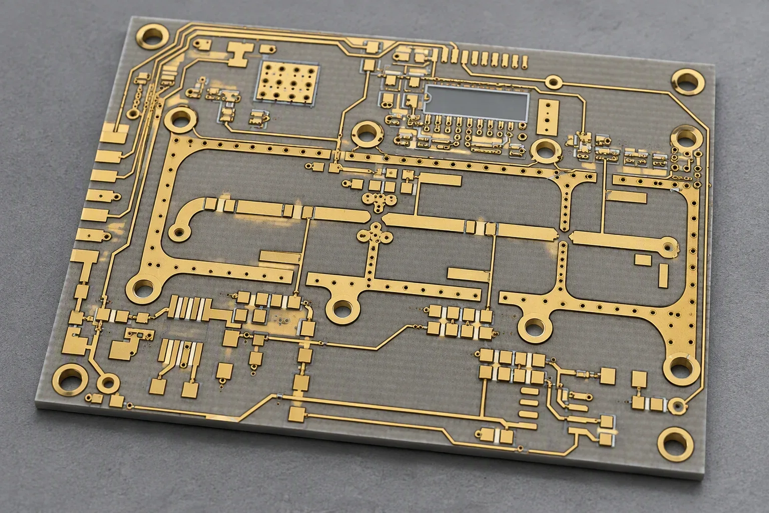
Controlled impedance for 8–20 layer network hardware
Network buyers screen suppliers on numbers, so here they are first:
impedance held to ±5% on premium builds and proved by a TDR coupon on every
lot, 2.5 mil line and space at the HDI grade, 0.1 mm laser microvias, and
stackups to 58 layers on request.
±5% TDR-verified2.5 mil line / space0.1 mm laser microviato 58 layers
Every one of these is visible in the design before the first panel
is laminated, and every one of them is cheaper to fix at quotation than after a
spin. They are also the three questions we ask first.
01
±10% window vs ±5%
A drifted pair closes the eye
A 100 Ω differential pair that sits at the edge of a ±10% window
has already spent the margin the SerDes was designed around, and the symptom
appears in the lab, not at the fabricator. The requirement therefore has to be
±5% measured on the finished board, with a coupon result that ships with
the panels.
02
8 – 20+ layer stackups
Back-drilling quoted as a special
Above a dozen layers the residual via stub starts to matter at 25G and beyond,
so the stackup needs back-drilling and stub control from the start. When a
fabricator treats that as an exception, the design gets re-spun around it,
which costs a schedule, not just a quotation.
03
802.3bt Type 4 ≈ 960 mA
Power over Ethernet sets the copper
The PoE class decides the copper plan before the signal layers do. 802.3af
Type 1 at 15.4 W is about 350 mA per pair and comfortable on
20 mil at 1 oz; 802.3at Type 2 at 30 W needs 25–35 mil;
802.3bt Type 4 at 90 W pushes roughly 960 mA across four pairs and
needs pours, matched via arrays and 2 oz copper. The hottest copper sits at
the RJ45/magjack outlet and the DC/DC input, not on the 48 V backbone.
The numbers we quote against
Impedance, stackup and materials in one table
This is the page a hardware engineer forwards internally. Every
value below is the manufacturing range we hold, and every impedance figure is
verified against a coupon rather than calculated and left at that.
Controlled-impedance and stackup range, telecom and networking builds
Parameter
In-house range
Notes
Single-ended impedance
50 Ω
Measured on a TDR test coupon at the board edge
Differential impedance
100 Ω
Ethernet pairs; other targets quoted from the stackup you specify
Impedance tolerance
±5% premium / ±10% standard
Verified per lot, with the coupon report filed against the lot number
Layer count
8 – 20 typical, to 58 on request
Low-loss layers hybridised into the FR-4 build
Board thickness
0.4 – 3.2 mm
Reference 8-layer build: 1.6 mm
Copper weight
0.5 – 20 oz
Reference 8-layer build: 1 oz signal, 2 oz planes
Materials
Rogers RO4350B (Dk 3.48 (specified as an absolute tolerance by the laminate supplier)), Isola 370HR (Dk 4.04), Megtron 6 (Dk 3.40), FR-4 hybrid
Loss figures quoted from the laminate supplier's datasheet for the grade ordered
Fine features
2.5 mil line / space, 0.1 mm laser microvia, 0.2 mm mechanical drill
Annular ring to 0.15 mm; aspect ratio and registration confirmed at engineering review
A reference stackup we laminate regularly: eight layers, 1.6 mm
overall, 1 oz on the signal layers and 2 oz on the planes, with the
impedance targets referenced to continuous planes. The cross-section below is the
same build the table above describes.
Reference 8-layer stackup, schematic, layer sequence and copper weights as built
Density and materials
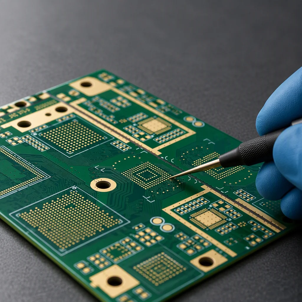
Fine-pitch routing and low-loss laminate side by side
High-density interconnect and low-loss material are usually bought
from two different suppliers. Here they are one build: the RF layers take the
low-loss laminate, the rest of the stack stays on FR-4, and the HDI layers carry
the escape routing.
2.5 mil line and space. The HDI grade, used for escape routing out of 0.25 mm-pitch BGA and for dense backplane connector fields.
0.1 mm laser microvia. Four-mil microvias with via-in-pad and filled-and-plated options, so a via does not have to be moved off the pad.
0.2 mm mechanical drill. The smallest mechanical hole we run, with annular ring held to 0.15 mm on the finished board.
01005 to 0.25 mm BGA. Mixed-density placement at ±25 µm accuracy, with 3D SPI confirming paste volume and alignment before reflow.
Press-fit connector holes. Plated through-holes sized and toleranced for compliant-pin connectors, with the insertion tooling agreed before the panel is released to drill.
Rogers and Taconic hybridisation. RO4350B at Dk 3.48 (specified as an absolute tolerance by the laminate supplier) on the RF layers, bonded into an FR-4 stack so only the layers that need low loss pay for it.
Verification and the carrier file
Ten gates, and the paperwork that travels with them
Carrier-grade buyers add a documentation requirement on top of the
ordinary inspection chain. For central-office equipment that means NEBS
Level 3 evidence, which is a filing burden before it is an engineering one.
The chain below is what runs on every networking order, and the record set is what
leaves with the carton.
01 IQC
Laminate, prepreg and bare boards checked on receipt, including the coupon on the panel border.
02 3D SPI
Koh Young paste inspection on volume, area, height and alignment; a violation forces a wipe and reprint.
03 3D AOI
Omron VT-RNS and SAKI BF-18D on 100% of boards across all nine SMT lines.
04 Digital X-ray
Nordson DAGE XD7600NT on a minimum of 5 pieces per lot, judged to J-STD-001.
05 Flying probe
Takaya APT-1500F with four heads: fixture-free electrical verification from the first article onward.
06 ICT
Agilent i3070 with up to 3,072 test points; a per-board pass or fail record is retained.
07 FCT
A product-specific fixture and script, developed with your engineering team, covering power-up and system behaviour.
08 FVI
Final visual inspection to IPC-A-610 Class 2 or Class 3 as ordered, with serial number and photographs.
09 OQC
Packaging, labelling, quantity and documents checked, sampled to AQL ANSI/ASQ Z1.4 (general inspection level II, single sampling, normal severity, AQL 0.65 for major defects).
10 Traceability
Board serialisation, photograph archive, material certificates and the coupon report filed per lot.
Record set shipped with a networking order, filed against the lot number
Application case
RF power amplifiers and antenna arrays
A project class rather than a product: X-band (8.6–9.6 GHz)
amplifier boards and four-element microstrip antenna arrays, where the laminate,
the copper and the mechanics are one design problem.
Requirement. Low-loss laminate under the RF path, impedance held at ±5%, a large coplanar copper area to carry heat away from the output devices, and a milled shield cavity that has to seat on the same board outline.
Solution. Low-loss layers were hybridised into an FR-4 stack so only the RF layers carry the premium laminate, the array feed network was dimensioned against a TDR coupon, and the shield cavity was assembled and inspected as part of the same build.
Outcome. Impedance verified per lot on the coupon, 100% AOI coverage, X-ray on a minimum of 5 pieces per lot at the shielded devices, and OQC sampled to AQL ANSI/ASQ Z1.4 (general inspection level II, single sampling, normal severity, AQL 0.65 for major defects) with the coupon report filed against the lot.
Send the Gerber with the layer assignment, the target impedance per
net class and the PoE budget. Prototype quantities of 5–50 pieces run in
5–10 days; series of 500–10,000 a year run on the same lines.