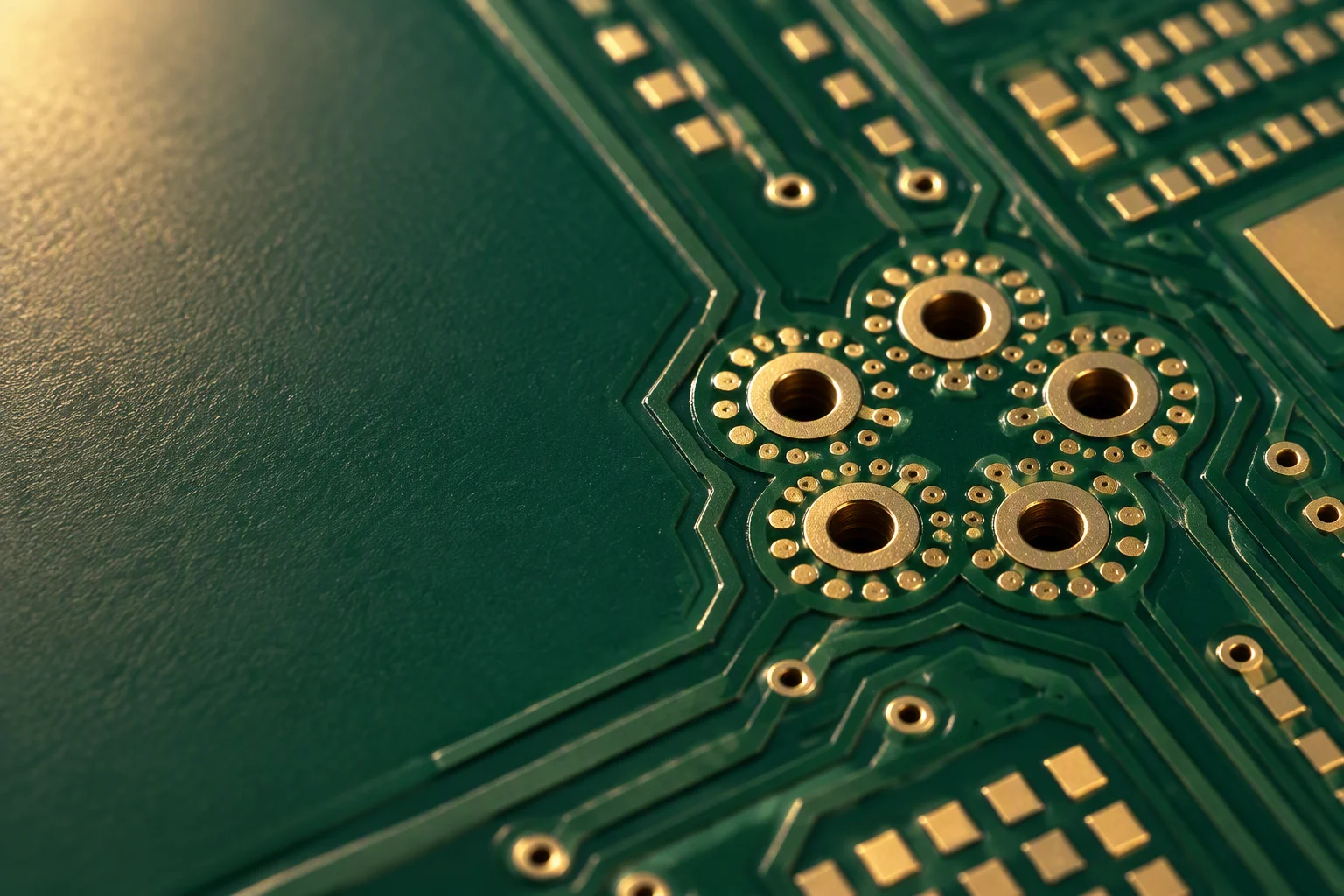
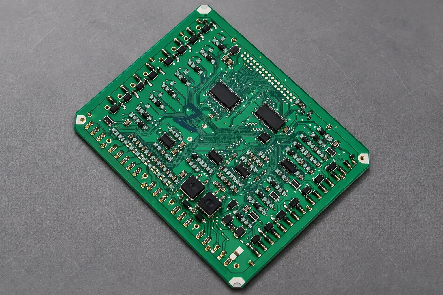
Microvia routing area
Stacked microvias at 0.1 mm inside a 0.25 mm pitch BGA footprint, with 2.5 mil escape routing between the pads.
Multilayer & HDI
Laser microvias at 0.1 mm (4 mil), mechanical blind and buried vias from 0.2 mm, and outer-layer features down to 2.5 mil. Stackups are quoted per project, and impedance is verified on a TDR coupon cut from the panel border rather than assumed from the drawing.
Stackup and parameter window
Layer count, finished thickness and copper weight are chosen together, because each one moves the press cycle and the drill programme. The window below is what the presses and lasers actually hold in production.
| Parameter | In-house window | How it is controlled |
|---|---|---|
| Layer count | 1 – 58 layers | 2–8 layers is the volume tier, 10–20 layers and HDI are quoted per project, and advanced builds run to 58 layers on request through extra lamination cycles |
| Board thickness | 0.4 – 3.2 mm | Finished thickness after lamination, plating and surface finish; the permitted drill-to-thickness ratio is confirmed at engineering review, per stackup |
| Copper weight | 0.5 – 20 oz | Outer and inner layers built to target; heavy copper starts at 3 oz (105 µm) and runs to 20 oz (700 µm) on the heavy-copper line |
| Laser microvia | 0.1 mm (4 mil) | Laser drilled through the outer dielectric, plated, then filled with conductive or non-conductive epoxy and planarised |
| Mechanical via | 0.2 mm | Blind and buried vias drilled and plated before the following lamination cycle; annular ring held to 0.15 mm (6 mil) |
| Line and space | 2.5 mil | Outer-layer HDI tier; inner layers normally released at 6 mil (0.15 mm) unless the impedance target demands tighter |
Sequential lamination
An HDI board is really two or three boards bonded to each other. Each extra cycle buys a layer of routing freedom and costs a registration step, so the sequence below is the order the work physically moves through the plant.
Core layers imaged and etched, then measured against the target copper weight and line width.
Cores, prepreg and foil bonded under press-cycle control; layer-to-layer registration is set at this step.
Microvias from 0.1 mm (4 mil) opened through the outer dielectric down to the first inner pad.
Conductive or non-conductive epoxy fills the microvia and the surface is planarised so via-in-pad can be placed on without the barrel wicking paste away from the joint.
Electroless copper followed by panel plating builds the barrels; copper is added until the target weight is reached.
The outer foil pair is bonded on top of the finished sub-assembly, closing the blind and buried via structure.
Pattern plating, etching and strip resist to 2.5 mil lines, with back-drilling where a stub would disturb the channel.
ENIG to IPC-4552, ENEPIG, OSP, immersion silver or tin, then electrical test and a TDR coupon read on the controlled nets.
Stackup cross-section
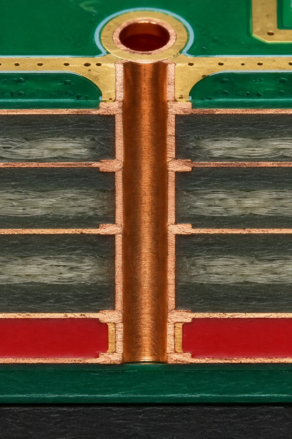
This is the same construction the table above describes, drawn to scale in the vertical direction only. Every value printed on the section, layer count, copper weight, via diameters, trace width, thickness and the impedance tolerance, matches the specification table on this page.
Microvia and via structures
Ask for the structure by name and the drill programme follows from it. All four can appear on the same board, which is why the stackup drawing matters more than the layer count alone.
Impedance control & TDR verification
Both tiers are measured the same way: a coupon on the panel border is probed with time-domain reflectometry, and the reading travels with the shipment. There is no version of this where the number is taken on trust.
| What is controlled | Standard builds | Premium builds | Verification |
|---|---|---|---|
| Single-ended trace impedance | ±10% | ±5% | TDR coupon on the panel border, read per lot |
| Differential pair impedance | ±10%, to 100 Ω | ±5%, to 100 Ω | TDR coupon, with the pair geometry recorded on the stackup drawing |
| What drives the tier | Standard dielectric builds and 6 mil line classes | Tighter line classes, low-loss laminate, or a channel budget that cannot absorb 10% | Agreed at DFM review, before the purchase order |
| Registration behind it | Layer-to-layer registration against targets on every cycle | Same, with additional coupon measurement on the controlled nets | Recorded against the lot number and shipped with the test report |
Reliability evidence
High layer-count boards fail at the interfaces: between glass bundles, between a barrel and its pad, between two lamination cycles. The checks below look at exactly those places.
HDI boards in production
Four views of the same construction: what the microvia field looks like on the surface, how the bonded layers read at the edge, how a filled via-in-pad sits under the mask, and how the array ships.
Stacked microvias at 0.1 mm inside a 0.25 mm pitch BGA footprint, with 2.5 mil escape routing between the pads.
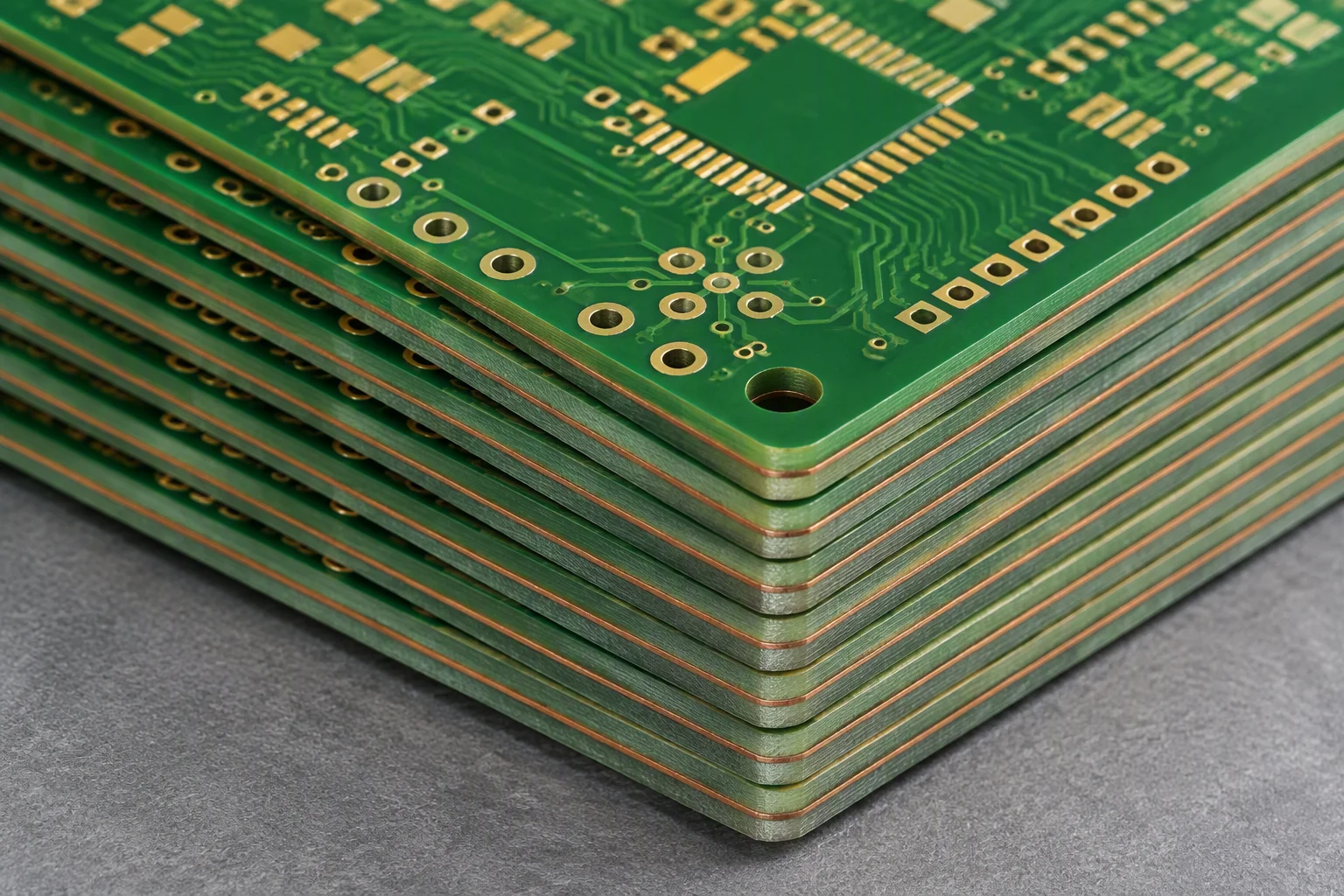
Bonded layers on edge after the second press cycle, checked for voids and registration before drilling begins.
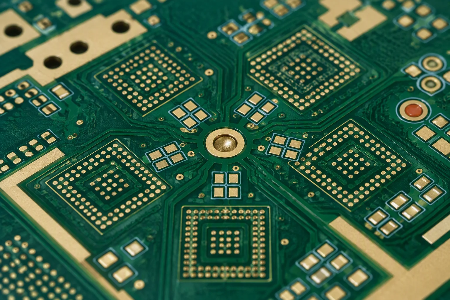
Microvias filled with conductive epoxy and planarised so the pad takes paste normally, 0.5–20 oz copper weight across the build.
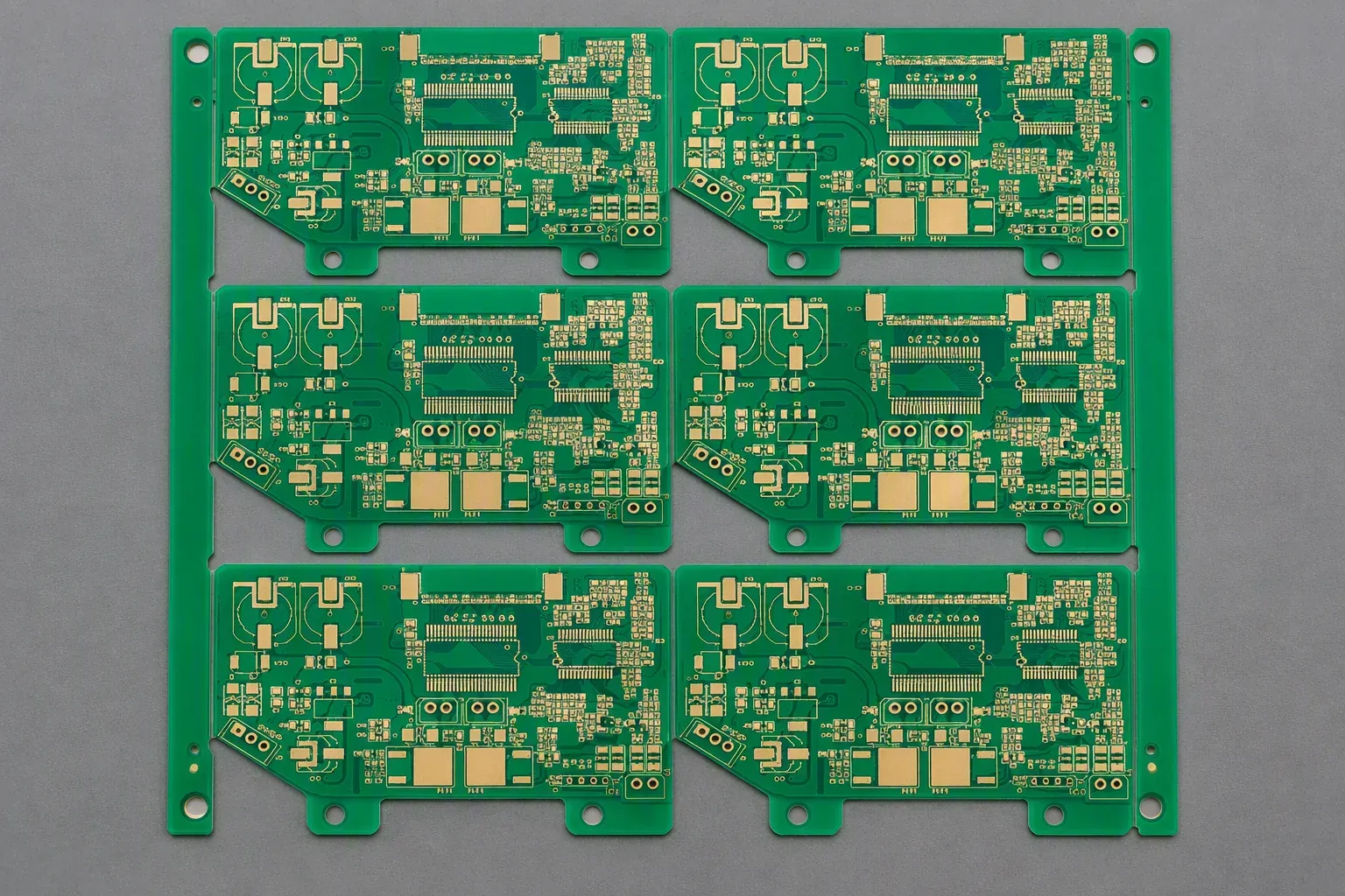
Six identical HDI circuits on one panel with tooling holes and routed tabs, impedance coupons placed on the border strip.
Quotation in 24 hours
Attach the layer assignment, the nets that must hit 50 Ω or 100 Ω differential, and any drill restrictions. An engineer confirms the construction and returns both lead-time brackets within one working day. NDA on request.
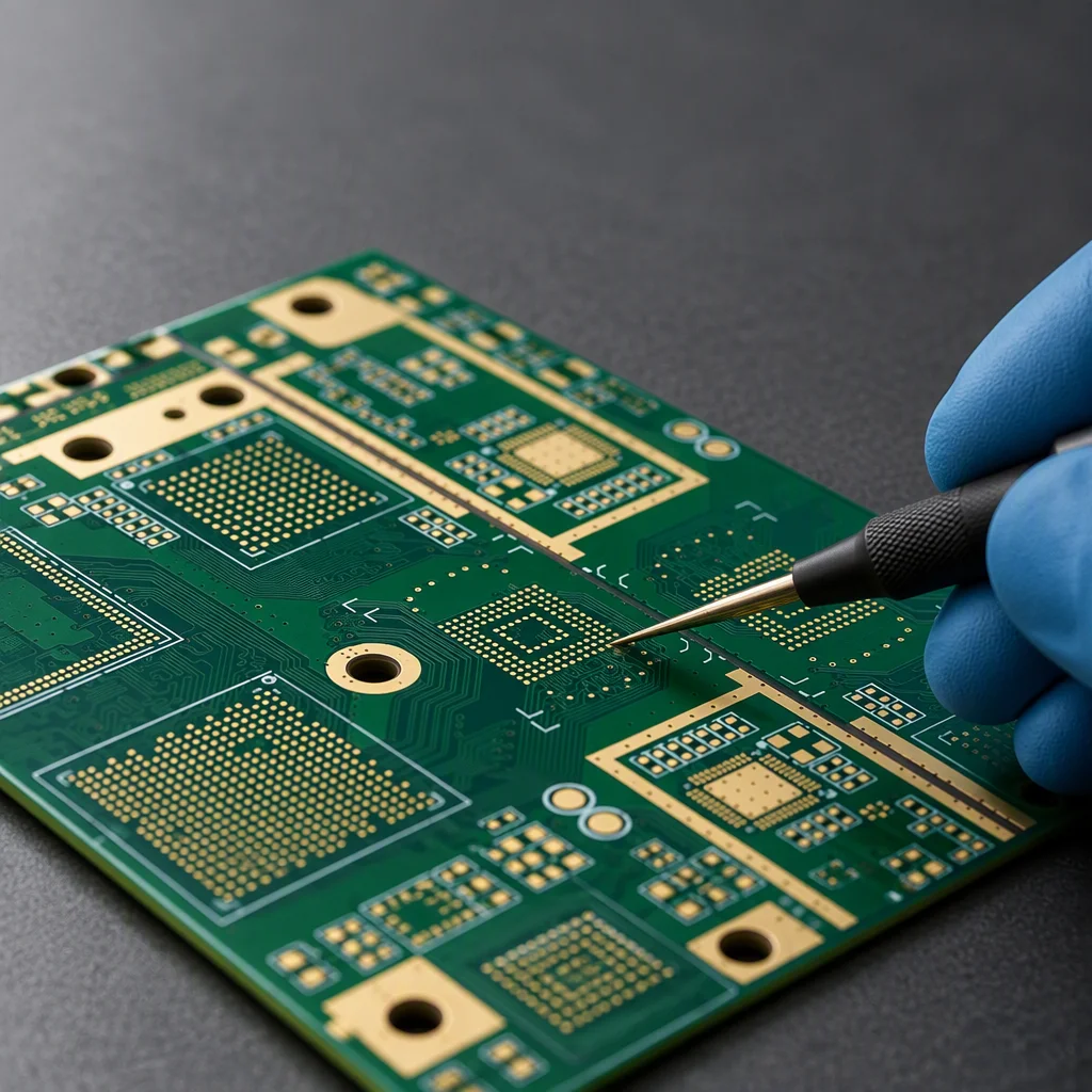
Send your Gerber, BOM or a plain description. An engineer, not a sales script, reviews it and replies within one working day. NDA on request.