Design guides & DFM
PCB design guides, DFM rules and templates
A working page for engineers, not a brochure. Accepted file formats, the numeric limits our process actually holds, a recommended-parameter table, six mistakes that cause rework, and a checklist to run before you submit.
What to send
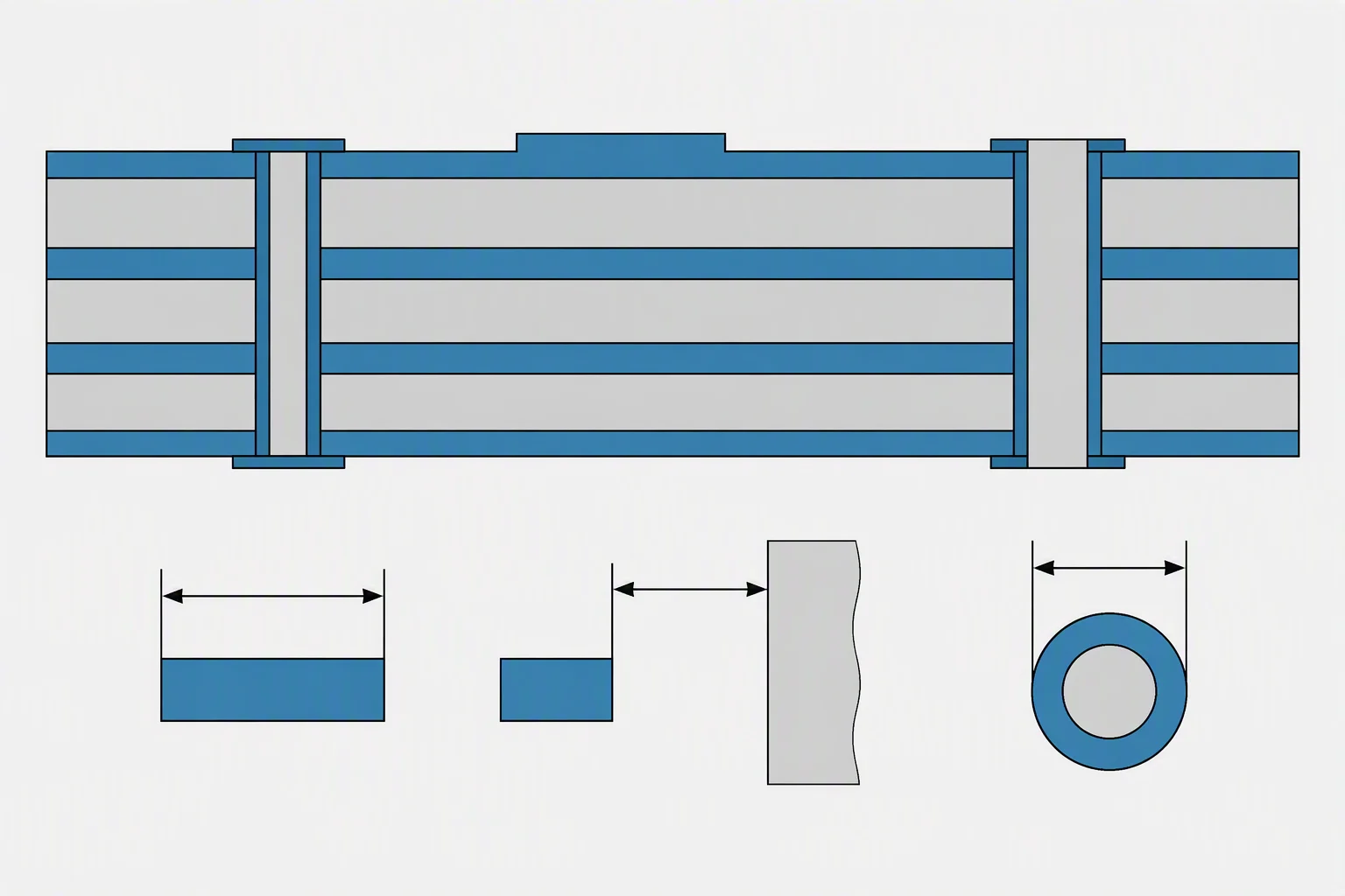
Eight things we need, and one we do not
Native CAD files are not required and we would rather not hold them. Data, drill and intent are enough, here is the full list.
DFM numeric rules
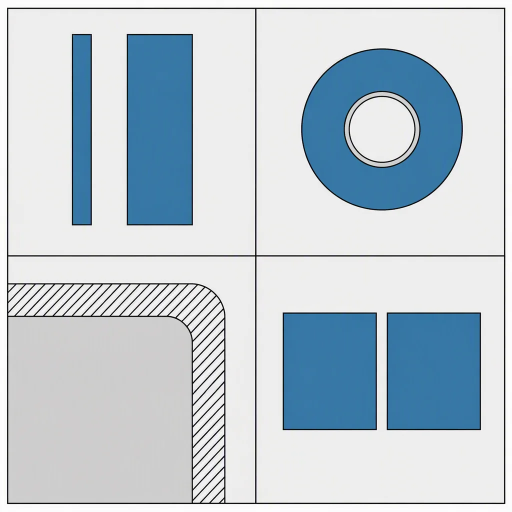
Sixteen limits you can check against
These are the numbers our process holds, split into fabrication geometry and design intent. Where a value depends on your hole size, layer count or board thickness, the rule says so instead of inventing a number.
| # | Rule | Limit |
|---|---|---|
| 1 | Minimum line width / space, standard multilayer | 4-6 mil |
| 2 | Minimum line width / space, HDI | 2.5 mil |
| 3 | Minimum mechanical drill | 0.2 mm |
| 4 | Minimum laser-drilled microvia | 0.1 mm |
| 5 | Minimum annular ring | 0.15 mm |
| 6 | Minimum solder-mask dam between pads | 0.1 mm |
| 7 | Silkscreen over a pad or mask opening | Not allowed |
| 8 | Board thickness range | 0.4-3.2 mm |
| # | Rule | Limit |
|---|---|---|
| 9 | Copper thickness range | 0.5-20 oz |
| 10 | Maximum board size, panel included | 600 × 1200 mm |
| 11 | Impedance control, stated in the stackup | ±10% std / ±5% premium |
| 12 | Component spacing outside the courtyard | Case by case |
| 13 | Panelisation: rail, tabs and tooling holes | Required |
| 14 | Fiducials per side, plus local ones per sub-board | 3 minimum |
| 15 | Thermal relief on pads connected to a plane | Spokes required |
| 16 | Via-in-pad treatment | Plugged and capped |
- Rule 1 and 2. 6 mil is the cost-optimal tier for standard multilayer; 2.5 mil needs an HDI stackup with laser microvias, so it changes both the layer build and the price.
- Rule 5. 0.15 mm is the floor. The ring each hole actually needs is confirmed hole by hole against its drill size and layer count at engineering review, and any hole that cannot hold the ring is flagged as a DFM risk before you receive a price.
- Rule 7. Legend ink on a pad or in a mask opening stops paste from wetting the copper. This is a hard rule, not a preference, and it is the single most common DFM note we raise.
- Rule 11. ±5% is a premium build verified by a TDR coupon on the board edge; ±10% is the standard tier. Write the target on the stackup drawing or in the Gerber notes, an impedance requirement that exists only in an email cannot be measured.
Recommended parameters
The choices that matter, in a standard tier and an advanced tier
Most boards should take the standard column. The advanced column exists for designs that need it, and it is priced accordingly.
| Parameter | Standard tier | Advanced tier |
|---|---|---|
| Layer count | 2-8 layers, the volume tier | 10-20 layers and HDI quoted per project; higher builds to 58 layers on request |
| Board thickness | 1.0-1.6 mm inside the 0.4-3.2 mm range | 0.4-3.2 mm with a controlled stackup and a TDR coupon |
| Copper thickness | 1 oz outer, 1-2 oz inner | 3 oz and above as heavy copper, up to 20 oz (700 µm) on power layers |
| Surface finish | Lead-free HASL, or OSP with a 6-month shelf life | ENIG to IPC-4552 (Ni 3-6 µm, Au 0.05-0.1 µm), ENEPIG, hard gold 150-200 HK25 for edge fingers |
| Laminate | FR-4, Tg 130-180 °C | High-Tg FR-4 at 170 °C or above, Rogers RO4350B, Isola 370HR, Megtron 6, aluminium IMS or polyimide |
| Impedance control | ±10%, verified by a board-edge TDR coupon | ±5% premium builds, differential pairs to 100 Ω |
| Panelisation | Rectangular panel with rails, breakaway tabs and tooling holes | Odd outlines with routed relief, V-cut or stamp holes, local fiducials on every sub-board |
| Delivery form | Bare boards, or assembled and tested | Turnkey with component sourcing, coating or potting, harness, sheet metal and box build |
Panelisation and process edge
The rule that gets skipped, and then costs money
Rules 13 and 14 in the table above are the ones that come back as a price increase or a broken board. The panel is not just your board copied five times. It is a handling fixture with its own geometry.
- Process edge. The conveyor and the machine rails need a strip along the panel edge that carries no components. State its width on the panelisation drawing, and plan the panel against the 600 × 1200 mm maximum including that strip.
- Breakaway tabs. Each sub-board is held by routed tabs, not by a continuous web. Where the tabs sit decides whether the board survives depanel, so their positions belong on the drawing rather than in a note.
- Tooling holes. Non-plated holes in the rail that locate the panel on the machine pins, put them in the drill file as non-plated, sized no smaller than the 0.2 mm mechanical drill floor.
- Fiducials. Three per panel side as a minimum, asymmetrically placed so the machine can tell which way the panel is loaded, plus local fiducials on each sub-board for fine-pitch placement.
- V-cut or stamp holes. Choose one. V-cut suits straight edges with a controlled remaining web; stamp holes suit odd outlines. Asking for both on the same edge is a DFM note every time.
Six common mistakes
Each one has a process consequence
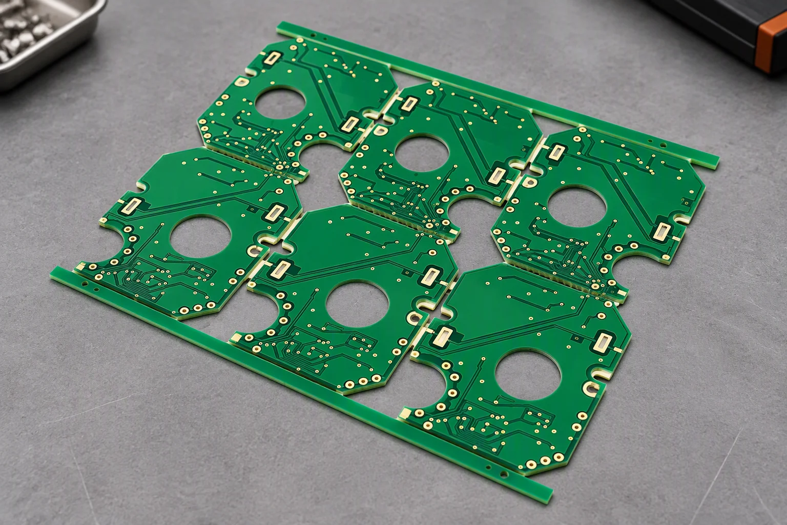
These six account for most of the DFM notes we raise. None of them is a matter of taste: each one breaks something specific downstream.
Legend printed over a pad
Ink in a mask opening stops paste from wetting the copper. The joint forms cold or not at all, and the board becomes a rework ticket at final visual inspection.
Via-in-pad without fill
An open via under a pad wicks paste away during reflow, so the joint starves. Rule 16 requires resin fill and a plating cap; if you cannot fill it, move the via out of the pad.
Panel without rails or tabs
The conveyor has nothing to grip and the depanel step cracks the edge. Rule 13 asks for a process edge, breakaway tabs and tooling holes on every panel.
Missing fiducials
The placement machine has no reference to calibrate against, so offset errors appear exactly where they hurt: 01005 passives and BGA at 0.25 mm pitch. Rule 14: three per side, plus local fiducials per sub-board.
Thermal pad tied straight into a plane
A solid connection to a large copper area drains heat out of the joint faster than the reflow profile can compensate, leaving an incomplete joint on a ground pad.
No courtyard clearance
Parts placed inside each other's courtyard leave no room for the nozzle or for rework. At 01005 and at 0.25 mm pitch BGA the required spacing is confirmed case by case rather than assumed.
Pre-submission checklist
Twelve boxes to tick before you send
Running this list takes ten minutes and typically removes one full engineering round trip from the quotation.
Templates and stackup notes
Send files, get the templates and a DFM report
There is no download form on this page and no second conversion path. Send your data through the same inquiry form the whole site uses, and the document set comes back with the engineering review.
Template pack, stackup suggestion table, impedance notes, panelisation and process-edge notes, a BOM template and this DFM checklist. Requested through the inquiry form, not a download button.
Stackup and impedance
Suggested layer builds for 4, 6 and 8 layers, with dielectric thickness, the impedance targets that sit on each signal layer, and the board-edge TDR coupon.
Panelisation and process edge
A drawing convention for rails, breakaway tabs, tooling holes and fiducials that matches rules 13 and 14, so the panel arrives at DFM review already dimensioned.
BOM and DFM checklist
A BOM template with the columns we need: including your acceptable alternates, and the twelve-item checklist from the section above.

DFM review and quotation in 24 hours
Send the Gerber. Get the DFM feedback.
Engineering review and quotation within 24 hours, with the DFM notes attached, not a price on its own.