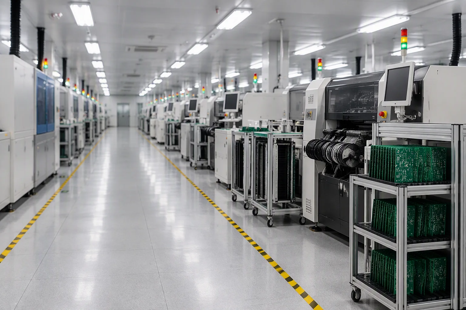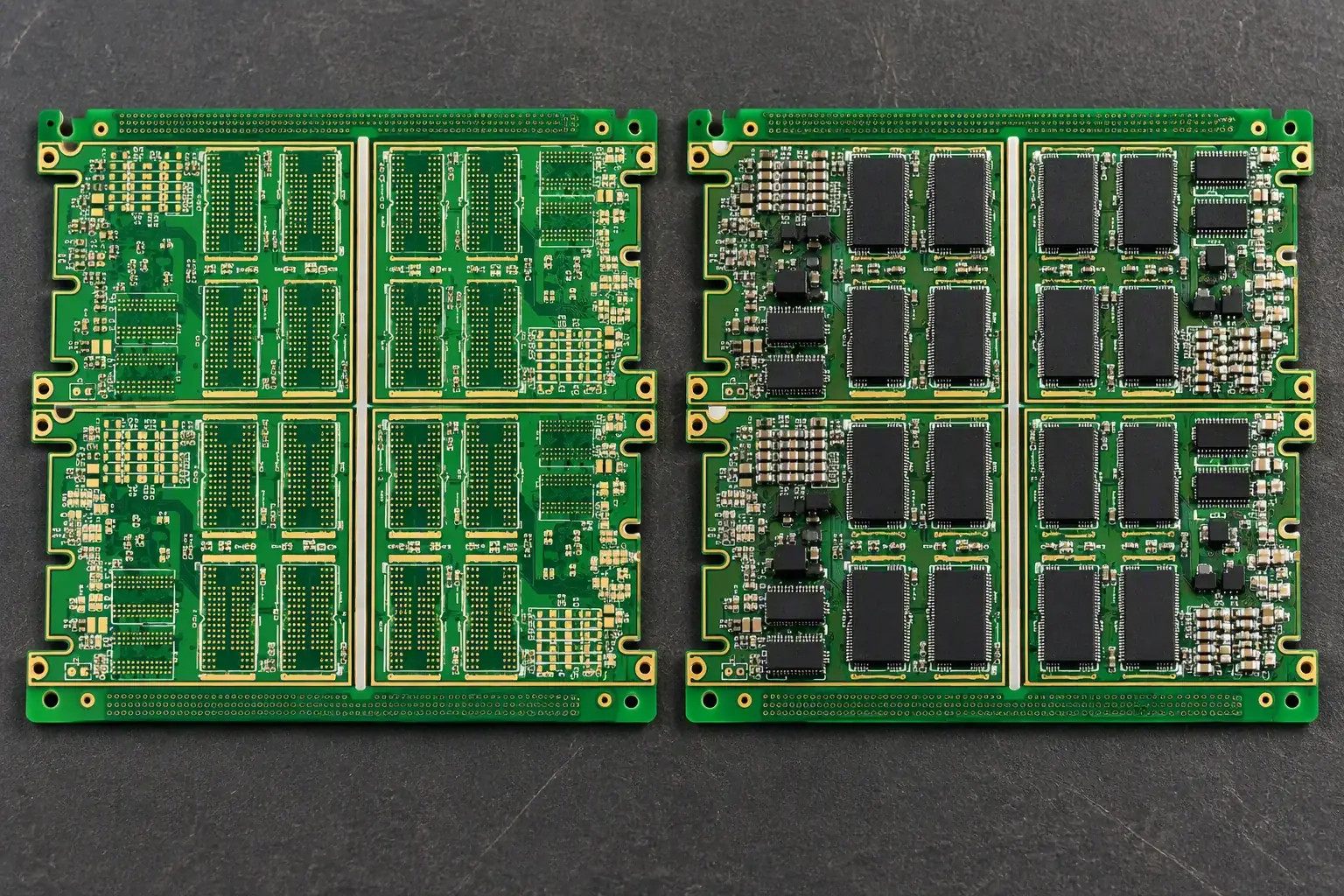
PCB vs PCBA: what actually changes
A bare board clears customs as HS 8534.00; an assembled board is classified by function. Different files, different test gates, different cost drivers, different risk.
Read the comparisonEngineering notes
Three working documents from the Shenzhen plant: what separates a bare board from an assembled one, how the SMT line runs in 2026, and the checklist an engineer should clear before releasing files.
Why these notes exist
Most supplier pages describe capability. These three notes describe decisions. What to specify, what a wrong specification costs, and what the factory does with the files once they arrive.
Between them the notes cover the questions that arrive with almost every quotation request: whether the supplier is pricing a bare board or an assembled board, which inputs each one needs, and which limits are hard. They touch the figures that decide a build, a layer range from 1 to 58, a 2.5 mil HDI trace floor against a 6 mil (0.15 mm) cost-optimal standard, a 0.2 mm minimum mechanical drill, and a 01005 component floor on the placement side.
Nothing here is decoration. Every figure is one we build to in Shenzhen: 9 SMT lines and 4–5 DIP lines feeding one quality system, 60+ export countries, no MOQ from a single board, and an engineering review with a quotation inside 24 hours. Where a value depends on your stackup, the note says so instead of guessing at a number.
The three notes
A bare board clears customs as HS 8534.00; an assembled board is classified by function. Different files, different test gates, different cost drivers, different risk.
Read the comparison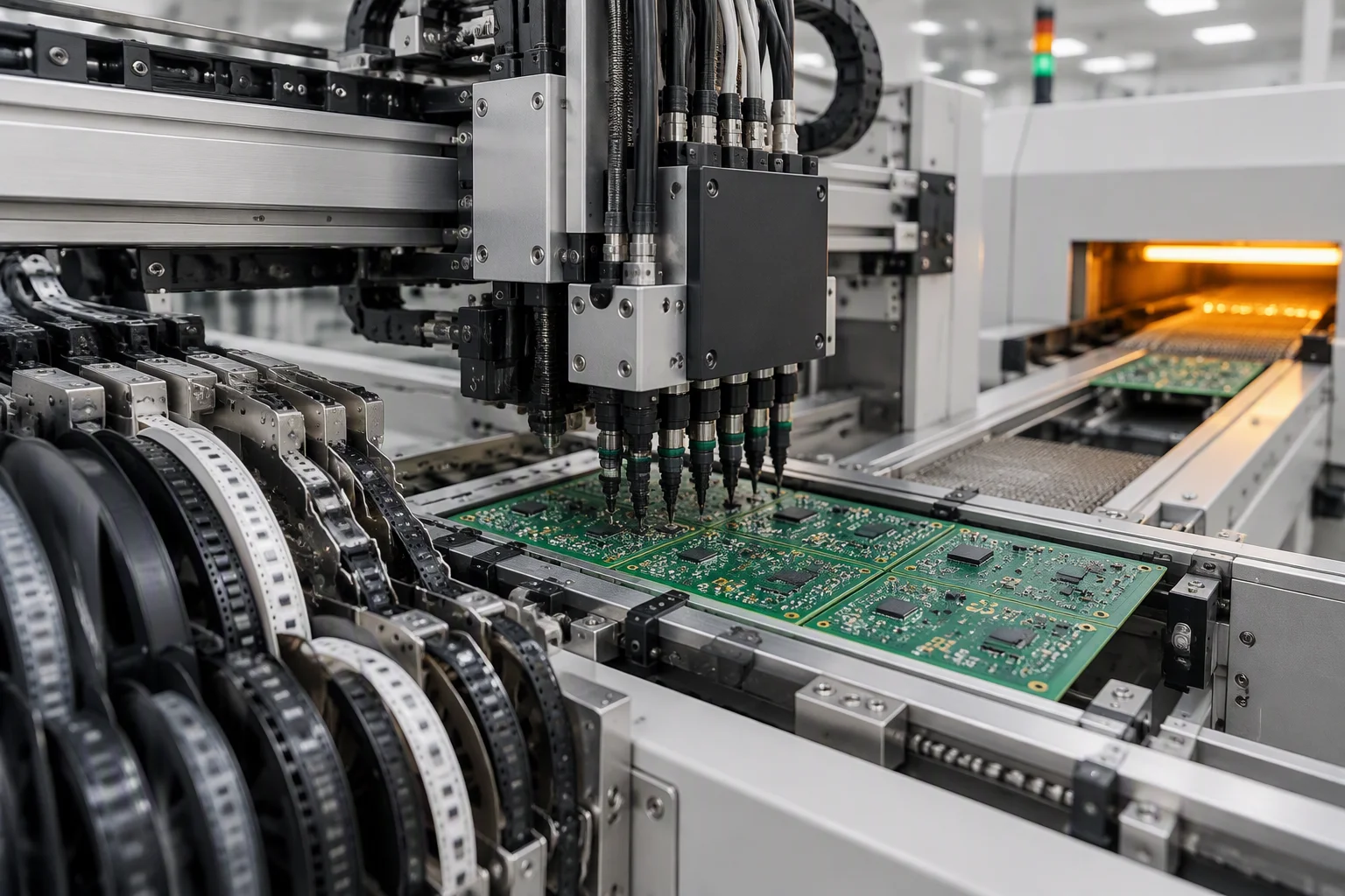
From paste printing and 3D SPI to placement at 80,000 CPH nominal, lead-free reflow at 245–260 °C, AOI on every board and X-ray on every lot.
Read the SMT guide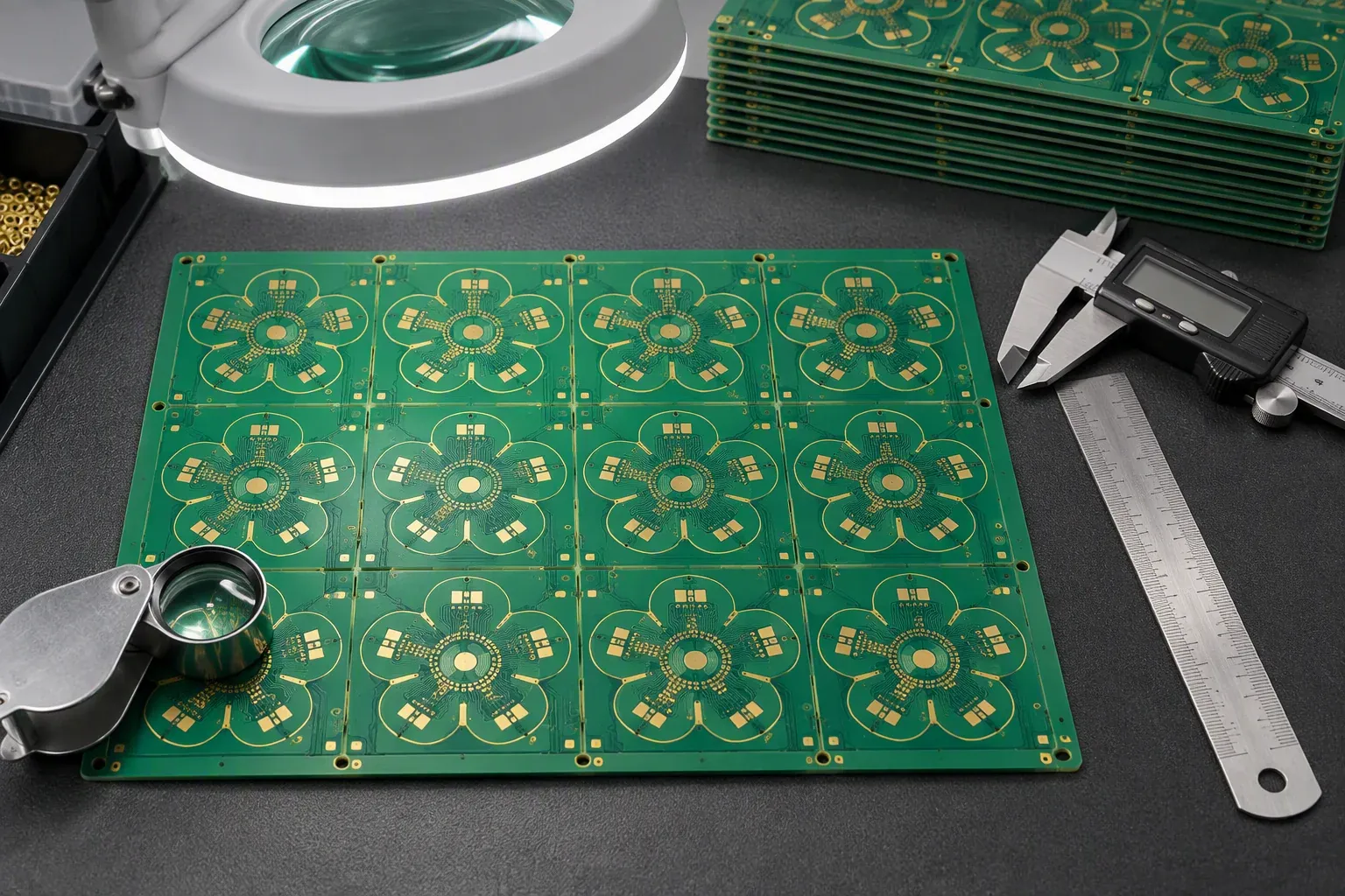
Stackup, copper, drills, solder-mask web, legend, panelisation, thermal limits and test access, with the numeric limit for every stage.
Open the checklistHow to use them
Decide whether you are buying a bare board or an assembled board. A fabrication quote starts from Gerber, ODB++ or IPC-2581 with a stackup; an assembly quote needs the BOM and the pick-and-place file as well.
Check the SMT guide against your own design: components from 01005 up to a 25 mm height, BGA to 0.25 mm pitch, an 8–12 zone reflow profile with a lead-free peak of 245–260 °C.
Run the DFM list stage by stage. The items that stop a build are rarely exotic: a 0.1 mm solder-mask web, a 0.2 mm mechanical drill, a fiducial the placement vision system cannot find.
Send Gerber, BOM and pick-and-place together. Engineering review and quotation come back inside 24 hours, and the DFM report is free before the PO. including on a five-piece prototype, because there is no MOQ.
Quotation in 24 hours
Gerber, BOM and pick-and-place are enough to start. An engineer reviews them and replies inside 24 hours with a price and a DFM report. No MOQ, no obligation to order.
Send your Gerber, BOM or a plain description. An engineer, not a sales script, reviews it and replies within one working day. NDA on request.