Comparison guide
PCB vs PCBA: what actually changes
A bare board and an assembled board are two products, two file sets, two cost structures and two customs classifications. Here is where each one starts and stops.
The short answer
One is a component. The other is a product.
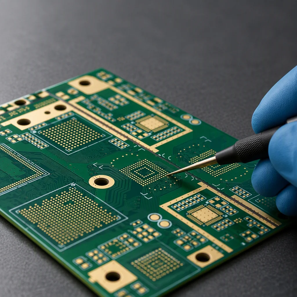
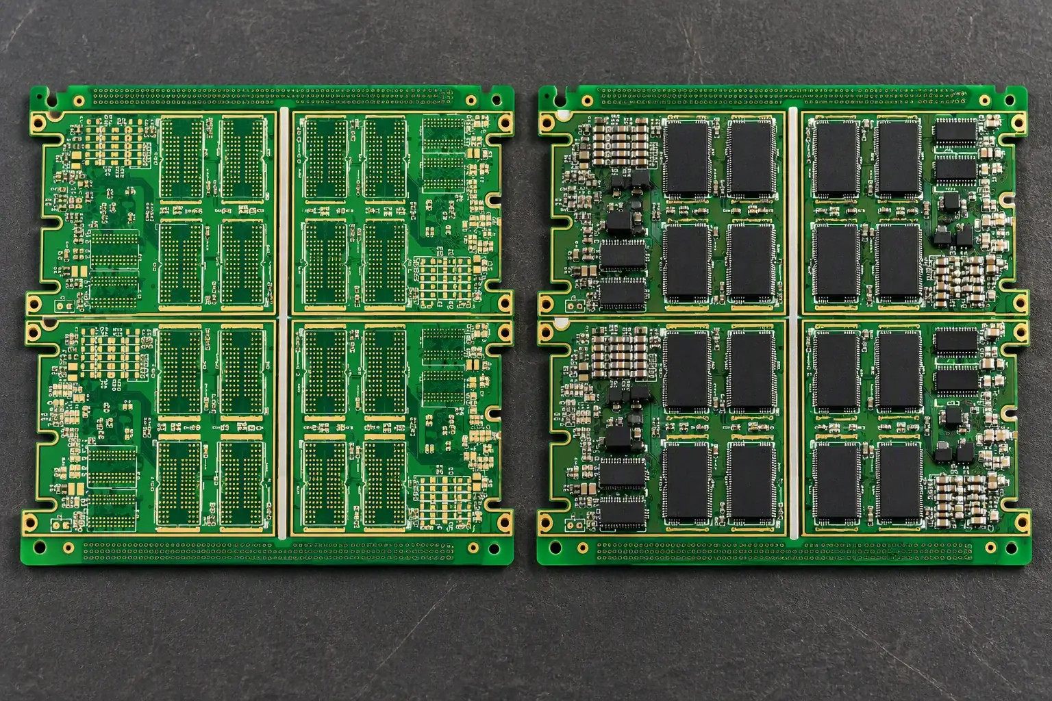
A PCB is the bare, unpopulated board: copper traces, drilled holes, plated barrels, a solder-mask layer and a legend, with nothing soldered to it. A PCBA is that same board after components have been placed, reflowed, inspected and tested. One is a part a contract manufacturer builds and ships in a box; the other is a working assembly that a distributor or an end customer receives and switches on.
The distinction is not academic. It changes the files an engineer has to prepare, the process that carries the cost, the tests that decide pass or fail, the lead time, and, at the border, the tariff line. Bare boards are classified under HS 8534.00. Assembled boards are classified by the function they perform: 8537.10 for boards that are parts of electrical control or distribution apparatus, 8538.90 for parts of apparatus of headings 8535 to 8537, 8517.62 for equipment that carries network traffic. Declaring an assembled board as 8534 is the most common customs error in this trade, and it is cheaper to catch it before the invoice than after it.
What follows separates the two so a quotation can be read for what it actually covers. Every figure is the range we build to in Shenzhen: 1–58 layers, 9 SMT lines and 4–5 DIP lines feeding one quality system, no MOQ, and engineering review with a quotation inside 24 hours.
Definitions
A bare board is judged as a part, an assembly as a circuit
One is measured against fabrication standards, the other against assembly standards. And the second one carries the test gates that decide whether a batch ships.
- Bare board: acceptance against IPC-A-600 and IPC-6012, plus electrical test and an impedance coupon where it applies
- Fabrication boundary: 600 × 1200 mm maximum laminate size, which is what panelisation has to respect
- Assembled board: acceptance against IPC-A-610 Class 2 or Class 3, with J-STD-001 governing the soldering
- Assembly precision: ±25 µm placement accuracy, from 01005 passives upward
Fabrication
What PCB fabrication actually does
Fabrication starts from a stackup. A 2-layer board in 1 oz copper with a finished thickness between 0.4 mm and 3.2 mm leaves the line as a passive structure; a 58-layer build with 20 oz (700 µm) copper and controlled impedance is a precision part in its own right. Inner-layer imaging, lamination, drilling, plating, outer-layer imaging, solder mask, surface finish and electrical test all run against IPC-6012 and IPC-A-600, and any build with an impedance requirement leaves with a TDR coupon measured at the board edge. ±10% as standard, ±5% on premium builds, differential pairs held to 100 Ω.
Minimum geometry is the first thing a quotation turns on. Our cost-optimal standard is a 6 mil (0.15 mm) trace and space; HDI builds go to 2.5 mil. Mechanical drilling bottoms out at 0.2 mm and laser-drilled microvias at 0.1 mm (4 mil), with a minimum annular ring of 0.15 mm (6 mil). Copper weight ranges from 0.5 oz to 20 oz, and heavy-copper work starts at 3 oz (105 µm).
Surface finish is the second cost lever, and it is a technical decision before it is a commercial one. ENIG, at Ni 3–6 µm plus Au 0.05–0.1 µm to IPC-4552, is the flat finish for BGA, fine pitch and RF. Lead-free HASL at 1–40 µm is the general-purpose option. OSP at 0.2–0.5 µm keeps a flat surface and a six-month shelf life. Hard gold at 150–200 HK25 survives more than 10,000 mating cycles on an edge connector. Laminate choice follows the same logic: FR-4 from Tg 130–180 °C for ordinary builds, high-Tg FR-4 at ≥170 °C when the assembly is lead-free, and Rogers RO4350B (Dk 3.48 (specified as an absolute tolerance by the laminate supplier)), Isola 370HR (Dk 4.04) or Megtron 6 (Dk 3.40) when the signal decides the stackup.
Two more numbers are worth knowing before a design is frozen. Solder mask runs in green, red, yellow, blue, white or black with a 0.1 mm minimum web between pads, and silkscreen needs 0.15 mm minimum line width with 0.8 mm minimum character height, a 1:5 ratio. Thermal qualification for the finished board is a 288 °C solder float for 10 seconds, the UL 796 and IPC-6012 measure.
Assembly
What assembly adds on top
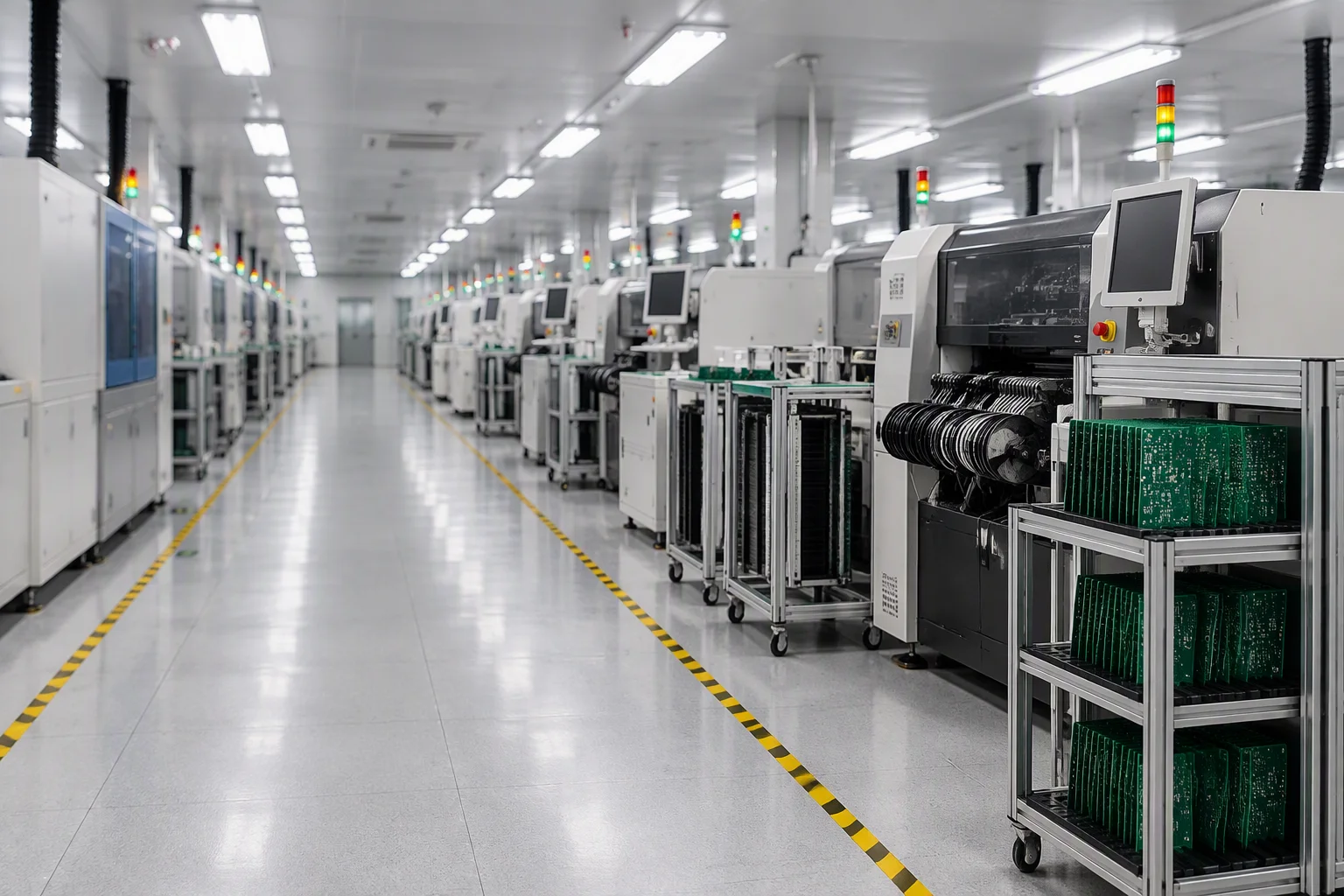
Assembly starts from a bill of materials rather than a stackup. The board is the substrate: paste is printed, parts are placed, the panel is reflowed, and the result is inspected and tested. Placement is where the capital sits, across nine SMT lines we run ASM SIPLACE X4iS platforms rated at 80,000 components per hour per line and Yamaha YSM20R machines at 72,000 CPH, both specified at ±25 µm. Those are nominal ceilings, not a schedule: real throughput depends on the board mix and the point count, and industry practice lands around 60% of the nominal rate.
What matters to a design is the range, components from 01005 and 0201 upward, BGA and µBGA to 0.25 mm pitch, fine pitch to 0.3 mm, and a 25 mm maximum component height on the SMT side. Feeding is not a constraint: reel, cut tape, tube, tray and bulk are all accepted. Through-hole content runs on 4–5 DIP lines with wave soldering, where the clearance is 120 mm above the board and 15 mm below it, plus programmable selective soldering, hand soldering and press-fit. Reflow ovens run 8–12 zones with a lead-free peak of 245–260 °C. The reason high-Tg laminate at ≥170 °C is not optional on a lead-free assembly.
Then comes the part that decides whether a batch ships. Three-dimensional SPI measures paste volume, area, height and alignment after printing and triggers an automatic wipe-and-reprint when a panel drifts out of specification. 3D AOI runs on 100% of boards on every SMT line, catching missing parts, reversed polarity, offset and tombstoning. Digital X-ray judges hidden BGA, QFN and LGA joints to J-STD-001 on a minimum of five boards per lot. In-circuit test covers up to 3,072 test points where a fixture is justified, and flying probe with four heads covers the builds that are not.
Inputs
The file set each one needs
A fabrication quotation can start from CAD data alone: Gerber RS-274X or 274D, ODB++, IPC-2581 or Eagle, plus drill data and a stackup. Mechanical detail travels as DXF or DWG, where the outline, cutouts, castellated edges and edge plating live.
An assembly quotation cannot start from CAD data alone. It needs the BOM in Excel or CSV, with manufacturer part numbers and reference designators, and the pick-and-place file in CPL or CSV. An assembly drawing as PDF or DXF removes the remaining ambiguity about orientation and about parts that are deliberately not placed. Anything missing becomes a manual engineering pass rather than a quotation. Which is why sending all of it at once is what makes a 24-hour answer realistic.
Cost and risk
Where the money and the exposure sit
On a bare board, cost is driven by area, layer count, copper weight, surface finish and how well the array uses the panel. With a 600 × 1200 mm maximum laminate size, panelisation is a money decision, not a formality. On an assembled board the board itself is often the smaller line item: component cost, procurement risk and the number of placement and test operations dominate the price.
Lead time splits the same way. A 2-layer bare board under 1 m² in quantities up to 50 pieces ships in 24 hours; 2- and 4-layer boards under 1 m² in five days, with a 48-hour expedite; 6–8 layers in seven days; 10 layers and above in ten. PCBA in the standard band runs 10–15 days, on a 50-unit build that is roughly 3–5 days of procurement, 4–7 days of board fabrication and 2–3 days of assembly and test, with a 5–7 day expedite available.
The risk that catches buyers is rarely the board. It is the material. In 2026, standard FR-4 laminate runs 6–8 weeks, MLCCs run 20–50+ weeks, and automotive MCUs and FPGAs run 52+ weeks. That is why every quotation we issue carries two columns: material in hand, and material on order. The second column is honest about the wait; the first is what an expedite can actually deliver.
Sourcing discipline belongs in the same conversation. We buy through authorised distribution by default, never through brokers or the spot market without the buyer's written approval, and material is traceable to date code and lot. Deviations and substitutions need written approval, and an NDA, non-use, non-disclosure, non-circumvention, can be signed before any file moves.
Customs
Two products, two tariff lines
A bare printed circuit board is HS 8534.00. It performs no function of its own, so the classification follows the goods. An assembled board takes the classification of the function it performs: 8537.10 for boards that are parts of electrical control or distribution apparatus, 8538.90 for parts of apparatus of headings 8535 to 8537, and 8517.62 for equipment that carries network traffic. Declaring an assembled board as 8534 is the most common error in the lane, and it is usually the buyer who owns the correction.
Two consequences follow. First, the origin document matters: a non-preferential certificate of origin issued through the chamber of commerce or customs, or an FTA or RCEP certificate where one applies. Second, the duty exposure follows the functional classification rather than the board classification. In the US market, assembled boards are normally classified by function, and the exclusion covering double-sided and four-layer rigid boards expires on 9 November 2026, when the rate moves from 12.5% to 37.5%. Tariff status as of September 2026.
We ship FOB Shenzhen by sea, FCA Shenzhen Airport by air, or on CIF, EXW and DDP terms where they fit; under DDP the buyer remains the importer of record, which is worth settling early rather than at the port. Documents travel with the goods: CoC, test report with ICT and FCT pass records, RoHS and REACH material declarations, packing list and commercial invoice. FAI reports, AOI and X-ray images and SPI data are available on request.
Comparison
Side by side, on the decisions a buyer makes
| Decision | Bare PCB | Assembled PCBA |
|---|---|---|
| What you receive | Unpopulated board: copper, mask, legend, surface finish | Board with components placed, soldered, inspected and tested |
| Minimum inputs | Gerber RS-274X/274D, ODB++ or IPC-2581, plus drill data and stackup | BOM (Excel/CSV), pick-and-place (CPL/CSV) and an assembly drawing |
| Governing standard | IPC-A-600, IPC-6012 | IPC-A-610 Class 2/3, J-STD-001 |
| In-house range | 1–58 layers, 0.4–3.2 mm, copper 0.5–20 oz | 9 SMT lines, 4–5 DIP lines, 01005 up, BGA to 0.25 mm pitch |
| Precision figure that matters | 2.5 mil HDI trace/space, 0.2 mm mechanical drill, 0.1 mm laser microvia | ±25 µm placement accuracy, reflow peak 245–260 °C |
| Quality gate | Electrical test and impedance coupon at the board edge | 3D SPI, 3D AOI on 100% of boards, X-ray on at least 5 per lot, ICT to 3,072 points |
| Standard lead time | 24 h for 2-layer up to 50 pcs under 1 m²; 5 days for 2/4-layer | 10–15 days, or 5–7 days expedited |
| Customs classification | HS 8534.00 | By function: 8537.10, 8538.90, 8517.62 |
| Where the risk sits | Stackup, surface finish and panel utilisation | Component availability, placement mix and test coverage |
Quotation in 24 hours
Tell us which one you are buying
Bare board, assembled board, or both in one order. Send Gerber, BOM and pick-and-place together and an engineer replies inside 24 hours with a price and a DFM report. No MOQ.