Process guide
SMT assembly in 2026, stage by stage
What happens to a panel between the stencil and the shipping box: nine gates, the equipment that runs them, and the limits that decide whether a design assembles cleanly.
The short answer
A sequence of gates, not a single operation
SMT assembly is a chain of measured gates. Paste is printed through a stencil, the print is measured in three dimensions, components are placed, the panel is reflowed, and the board is then inspected optically, radiographically and electrically. Any gate can stop a panel, and every gate leaves a record that travels with the batch. Which is why the process is worth reading as a sequence rather than as a list of machines.
The 2026 version of that sequence runs at 80,000 components per hour nominal per line on our ASM SIPLACE X4iS platforms, at ±25 µm accuracy, across nine SMT lines. Before reflow there is 3D SPI on the print; after reflow there is 3D AOI on 100% of boards on every line, digital X-ray on at least five boards per lot, and in-circuit test up to 3,072 test points on the builds that justify a fixture. Through-hole content runs on 4–5 DIP lines with wave and selective soldering.
What follows is that flow with the numbers attached, so a design can be checked against the process before the files are released rather than after the first panels come off the line.
How to read this
Nine gates between the stencil and the box
Each stage below names the limit that applies to it, so a design can be checked against the process rather than against a brochure.
- Stages 01–02: stencil printing, then 3D SPI measuring paste volume, area, height and alignment on every panel
- Stages 03–04: placement at 80,000 CPH nominal per line and ±25 µm, then an 8–12 zone lead-free reflow at 245–260 °C
- Stages 05–07: 3D AOI on 100% of boards, X-ray on at least 5 boards per lot, electrical test to 3,072 points
- Stages 08–09: recorded rework, IPC-A-610 Class 2/3 final visual, AQL ANSI/ASQ Z1.4 (general inspection level II, single sampling, normal severity, AQL 0.65 for major defects) outbound sampling
Flow
The line, stage by stage
| # | Stage | Equipment or method | What it controls |
|---|---|---|---|
| 01 | Solder-paste printing | Laser-cut or electroformed stencil | Aperture fill, print repeatability, paste deposit per pad |
| 02 | 3D SPI | Koh Young | Paste volume, area, height and alignment; out-of-spec panels are wiped and reprinted |
| 03 | Placement | ASM SIPLACE X4iS; Yamaha YSM20R | 80,000 CPH nominal per line, ±25 µm, 01005 up to 25 mm component height |
| 04 | Reflow | 8–12 zone oven, lead-free | Peak 245–260 °C, profile matched to paste and laminate |
| 05 | 3D AOI | Omron VT-RNS; SAKI BF-18D | 100% of boards on every SMT line: missing parts, polarity, offset, tombstoning, joints |
| 06 | Digital X-ray | Nordson DAGE XD7600NT | Hidden BGA, QFN and LGA joints to J-STD-001; minimum 5 boards per lot |
| 07 | Electrical test | Takaya APT-1500F flying probe; Agilent i3070 ICT | Opens, shorts, component values, diode orientation, IC connectivity; up to 3,072 points |
| 08 | Rework and touch-up | Hand soldering, programmable selective soldering, press-fit | Repair to the same acceptance standard as the original joint, recorded per board |
| 09 | Final and outbound | IPC-A-610 Class 2/3 visual; AQL ANSI/ASQ Z1.4 (general inspection level II, single sampling, normal severity, AQL 0.65 for major defects) sampling | Inspection stamp, serial number where required, photo archive, packing and documents |
Stages 01–02
The stencil decides the rest
Printing is a low-cost stage to get right and an expensive one to get wrong, because every downstream defect starts as a paste deposit. Stencils are laser-cut or electroformed, and the aperture geometry decides how much paste lands on each pad. After printing, a 3D SPI system measures volume, area, height and alignment pad by pad, not by eye and not by sampling. When a print drifts outside its limits, the line wipes the stencil and reprints instead of reflowing a bad print, and the SPI report can be issued per array so the print distribution is visible rather than reduced to a pass mark.
Small features raise the stakes. A 01005 chip or a 0.3 mm fine-pitch lead needs a print that repeats across the whole panel, and a BGA at 0.25 mm pitch needs paste volume that is predictable enough to form a joint without bridging. Both are printing problems long before they are reflow problems.
Stage 03
Placement capability in 2026
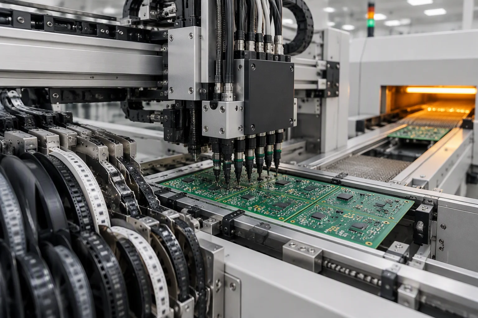
Our placement fleet runs ASM SIPLACE X4iS platforms rated at 80,000 components per hour per line and Yamaha YSM20R machines at 72,000 CPH, both specified at ±25 µm accuracy. The nominal rate is a ceiling rather than a schedule: boards with many small parts, tray-fed connectors and 25 mm-tall components run slower, and industry practice lands near 60% of the nominal figure. What a design actually depends on is the range and the feeding. Components load from reel, cut tape, tube, tray and bulk, and the machine set covers 01005 and 0201 passives upward, BGA, µBGA, CBGA, QFP, QFN, LGA, CSP and PoP, with BGA to 0.25 mm pitch and fine pitch to 0.3 mm.
Board size is the one placement figure that is confirmed per project rather than published as an absolute: conveyor-class SMT lines typically accept 510 × 460 mm, and anything beyond that is quoted against the specific line instead of assumed. Component height is capped at 25 mm on the SMT side. On the through-hole side, wave soldering needs 120 mm of clearance above the board and 15 mm below it, which is the number that decides whether a tall capacitor or a heatsink can go through that route at all.
Stage 04
Reflow, and why 245–260 °C is the number to know
Reflow ovens run 8–12 zones so the profile can be shaped rather than merely heated: preheat, soak, reflow, cool. For lead-free paste the peak sits between 245 °C and 260 °C. That temperature turns laminate choice and moisture control into assembly decisions rather than purchasing ones. High-Tg FR-4 at ≥170 °C is the baseline pairing for a lead-free build, and standard FR-4 in the Tg 130–180 °C band has to be checked against the actual profile rather than assumed to be fine.
Moisture is the second half of the same problem. Components ship in an ESD shielding bag inside a moisture-barrier bag with desiccant, a humidity indicator card and a dry-pack label that states the MSL level and the seal date, vacuum sealed and stored below 40 °C and 90% RH. Floor life after opening follows J-STD-020: 168 hours at MSL3, 72 hours at MSL4, 48 hours at MSL5 and 24 hours at MSL5a. When the clock runs out, a 125 °C bake brings MSL3 parts with bodies of 1.4 mm or less back in roughly nine hours. Popcorning is not a reflow problem; it is a storage and scheduling problem that surfaces at reflow.
Stages 05–07
What is checked, and on how many boards
Coverage is the part of an inspection claim worth reading, because "AOI inspected" means very little on its own. Our rule is three independent inspections per product per batch: in-line optical inspection, electrical test, and final visual inspection. With X-ray layered on top wherever a joint is hidden.
| Gate | Coverage | What it verifies |
|---|---|---|
| IQC incoming | Per lot | Bare-board visual and dimensional check plus test coupon; component date code, quantity and solderability |
| 3D SPI | Every printed panel | Paste volume, area, height and alignment; out-of-spec panels are wiped and reprinted |
| 3D AOI | 100% of boards, all SMT lines | Missing parts, polarity, offset, tombstoning and joint quality; industry data puts AOI capture at 85–95% of placement, bridging and missing-part defects |
| Digital X-ray | Minimum 5 boards per lot | Voiding, ball shape and bridging on BGA, QFN and LGA joints, judged to J-STD-001 |
| ICT | Per board where a fixture is justified | Opens, shorts, resistor and capacitor values, diode orientation, IC connectivity; up to 3,072 test points, pass/fail archived per board |
| FCT | Per board on custom fixtures | Power-up, signal integrity, firmware programming, system-level verification; scripts developed with the customer's engineering team |
| FVI final visual | 100% | IPC-A-610 Class 2 or Class 3; inspection stamp, serial number where required, digital photo archive |
| OQC outbound | AQL ANSI/ASQ Z1.4 sampling | Packing, labels, quantity and accompanying documents: CoC, test report, packing list |
Read the coverage column as a design constraint rather than a service list. A BGA with hidden joints is only as verifiable as the X-ray and boundary-scan access the layout allows; a board with no probe points falls back to flying probe, which programs faster than a fixture but tests slower per unit. Both routes are workable, but the choice is made in layout, not in production.
Stage 08
Rework, records and the corrective loop
Rework is part of production, provided it is recorded. Hand soldering, programmable selective soldering, press-fit and rework of area-array packages all run to the same acceptance standard as the original joint, and boards are serialised where the customer's process requires it, with digital photographs archived per lot. Conformal coating, potting, ultrasonic and DI water cleaning, box build, cable harnesses and sheet metal close the back end of the line when the product needs them; the coating spec we work to is IPC-CC-830B, from acrylic at 25–75 µm through to parylene at 5–50 µm.
The corrective side is procedural rather than improvised: monthly quality review, 8D or CAPA corrective actions where a defect repeats, an annual internal audit, and material certificates travelling with the shipment. More than 500,000 products delivered to 150,000+ customers sit behind that process, and ESD handling across the plant follows ANSI/ESD S20.20.
Getting a quote
Three files, one engineering review
An SMT quotation needs three things: the Gerber set in RS-274X or 274D, ODB++ or IPC-2581; the BOM in Excel or CSV with manufacturer part numbers and reference designators; and the pick-and-place file in CPL or CSV. An assembly drawing as PDF or DXF removes ambiguity about orientation and about parts that are deliberately not placed. That is enough for an engineering review, a DFM report and a price inside 24 hours, and the DFM review is free before the purchase order. There is no MOQ, so a five-piece prototype and a 50,000-piece series pass through the same gates.
Two commercial notes belong in the same email. Component sourcing defaults to authorised distribution with traceability to date code and lot, and no broker or spot-market parts are used without the buyer's written approval. Lead time is quoted in two columns, material in hand and material on order, because in 2026 standard FR-4 laminate runs 6–8 weeks, MLCCs 20–50+ weeks and automotive MCUs or FPGAs 52+ weeks. Expedited assembly is 5–7 days once material is on the floor, against a standard band of 10–15 days.
Quotation in 24 hours
Send the BOM. Get a process plan.
Gerber, BOM and pick-and-place are enough. An engineer checks the design against the nine lines and replies inside 24 hours with a price, a DFM report and a lead time in two columns.