PCB fabrication & PCBA assembly · Shenzhen · since 1998
PCB fabrication and PCBA assembly, built in Shenzhen since 1998
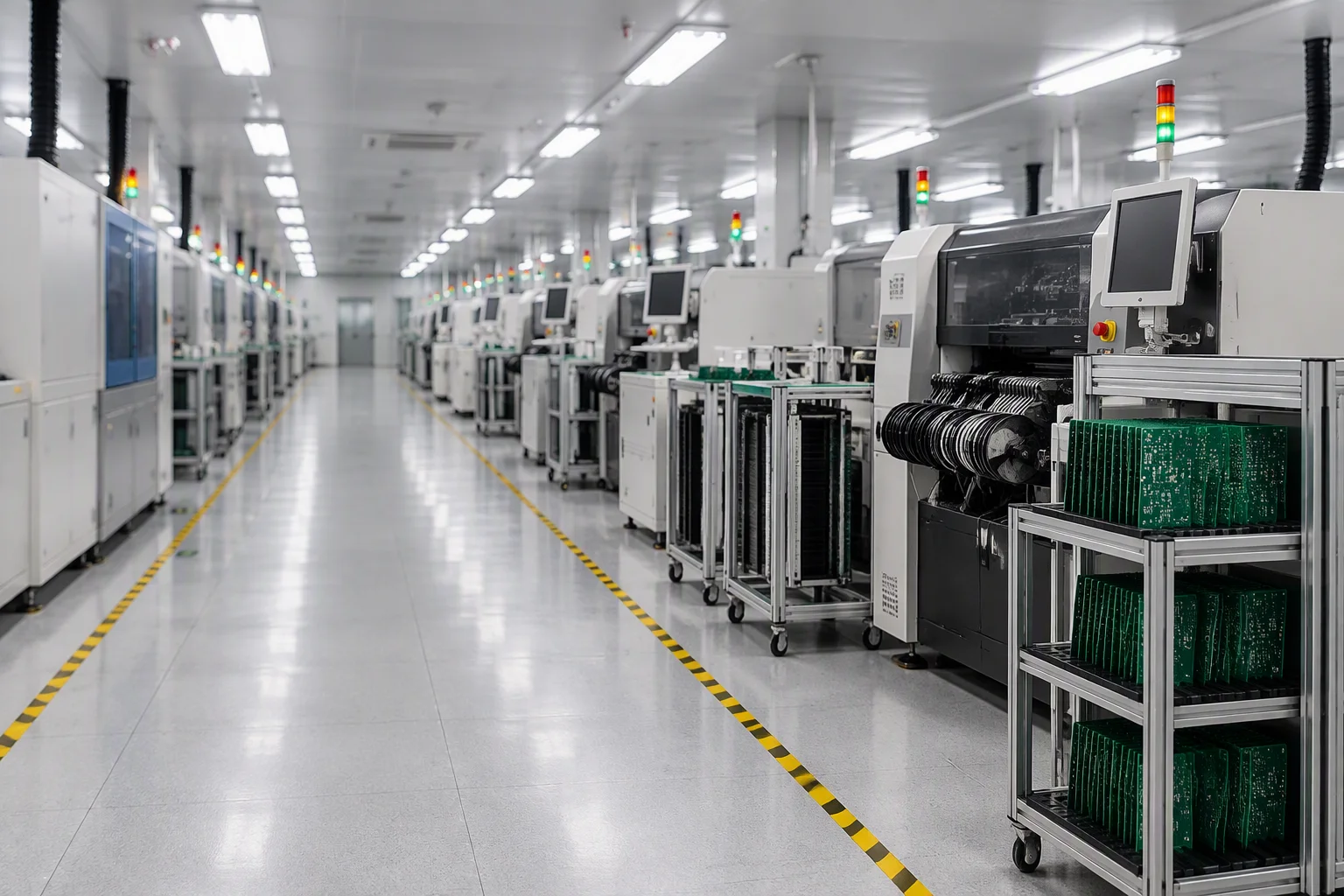
One factory takes your Gerber, BOM and pick-and-place file from bare board to boxed product: 1–58 layers, 9 SMT lines, 4–5 DIP lines and no MOQ. An engineer reviews the files and answers with a price inside 24 hours.
Scale, in numbers
Process, quality and inspection
The numbers your design has to fit inside
One page carries all three: the three process windows we run, the quality system those windows sit under, and the inspection chain that decides whether a board ships. Every figure on it comes from a machine on our own floor.
Industries
Eight industries, eight sets of process rules
The board is the same; the rules are not. Each industry below carries its own laminate, copper, coating and documentation requirements into the same nine lines.
Engineering & DFM
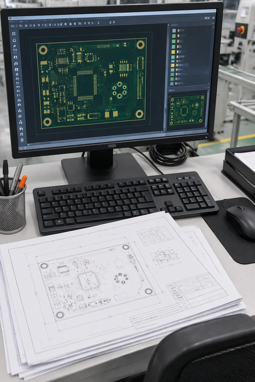
The DFM report arrives before the purchase order
Engineers, not account managers, read your files. The review is free, it happens before you commit, and it is written in the language of your fabrication drawing.
- Files we take as-is: Gerber RS-274X or 274D, ODB++, IPC-2581 and Eagle for the board; BOM in Excel or CSV plus a pick-and-place file in CPL or CSV; DXF or DWG for the outline. No CPL? We build it from the Gerber and confirm rotations with you.
- Checked before release: annular ring (0.15 mm minimum), solder-mask bridge (0.1 mm minimum), silkscreen legibility (0.15 mm line, 0.8 mm character height at 1:5), via-in-pad and filled vias, castellated edges, and panelisation inside a 600 × 1200 mm working area.
- Stackup and impedance: ±10% standard, ±5% on premium builds, verified with TDR coupons on the board edge. Rogers RO4350B, Isola 370HR and Megtron 6 are held for controlled Dk, differential pairs to 100 Ω.
- Response inside 24 hours: a quotation plus the questions that decide cost: usually panel utilisation, solder-mask colour, finish and the test strategy you want built into the price.
How an order runs
Six steps from files to freight
The clock is honest about 2026 material reality: sourcing is quoted separately from manufacturing, and both numbers appear in the same quotation.
Files in, questions out
Send Gerber, BOM and pick-and-place. An engineer reads them and comes back inside 24 hours with a quotation and the blocking questions, no sales script, no waiting for a "review meeting".
Free DFM and stackup sign-off
Before the purchase order: annular ring, mask bridge, silkscreen, panelisation, via-in-pad and impedance coupons checked and returned as a written report you can forward internally.
Component sourcing
Authorised channels first, from 5,000+ verified suppliers. Long-lead parts are flagged immediately: FR-4 laminate 6–8 weeks, MLCC 20–50+ weeks, automotive MCU and FPGA 52+ weeks.
PCB fabrication
1–58 layers laminated in-house, 2–8 layers on the standard band. Two-layer boards of 50 pcs or fewer under 1 m² ship in 24 hours; 6/8 layers take 7 days and 10+ layers 10 days.
SMT, DIP and test
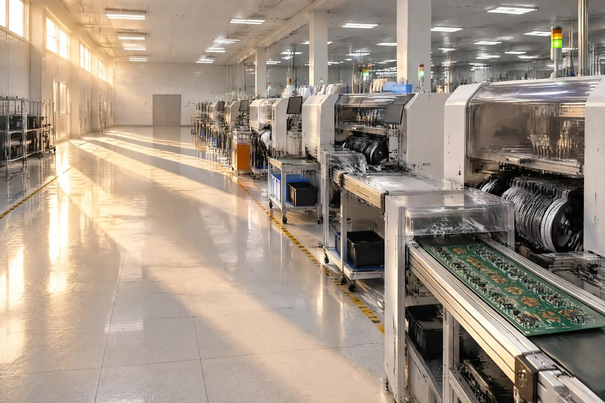
Nine SMT lines and 4–5 DIP lines, lead-free reflow at a 245–260 °C peak, 3D AOI on every board, then flying probe, ICT on 3,072 test points, or functional test to your own script.
Pack, documents, freight
ESD shielding bags inside MBB dry packs with desiccant and a humidity indicator card; CoC, test report and material declarations in the carton. PCBA typically 10–15 days, expedited 5–7 days, then FOB Shenzhen or FCA Shenzhen Airport.
Quotation in 24 hours
Send the Gerber. Get a price and a DFM report.
No MOQ, one board or fifty thousand, on the same nine lines. Files stay under NDA on request, and an engineer answers every message.